


SPI master and slave mode
SPI signal wire
SPI equipment selection
SPI data sending and receiving
Four modes of SPI communication
Communication protocol for the SPI
Three modes of the SPI
SPI Schematic connection
The SPI initialization configuration in STM32
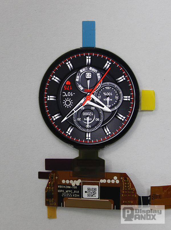
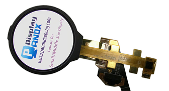
SPI Display Panel From Panox Display
What is SPI ?
SPI stands for Serial Peripheral interface and, as the name suggests, a serial peripheral interface. Motorola was first defined on its MC68HCXX-series processors.SPI is a high-speed, full-duplex, synchronous communication bus, and only occupy four lines on the chip pin, saving the pin of the chip, while saving space for the PCB layout, providing convenience, mainly used in EEPROM, FLASH, real-time clock, AD converter, and between the digital signal processor and digital signal decoder.
SPI master and slave mode
The SPI has two master and slave modes. An SPI communication system needs to include one (and only one) master device and one or more slave devices. The main device (Master) provides the clock, the slave device (Slave), and the SPI interface, which are all initiated by the main device. When multiple slave devices exist, they are managed by respective chip signals.
The SPI is a full-duplex, and the SPI does not define a speed limit, and the general implementation can usually reach or even exceed 10 Mbps
SPI signal wire
The SPI interface generally uses four signal lines for communicating:
SDI (Data Entry), SDO (Data output), SCK (Clock), CS (Select)
MISO: Primary device input/output pin from the device. The pin sends data in the mode and receives data in the main mode.
MOSI: Primary Device Output/input pin from the device. The pin sends data in the main mode and receives data from the mode.
SCLK: Serial clock signal, generated by the main equipment.
CS / SS: Select signal from the equipment, controlled by the main equipment. It functions as a "chip selection pin", which selects the specified slave device, allowing the master device to communicate with a specific slave device alone and avoid conflicts on the data line.
Four lines are used on the hardware.MOSI: Primary Device Output/input pin from the device. The pin sends data in the main mode and receives data from the mode.
SCLK: Serial clock signal, generated by the main equipment.
CS / SS: Select signal from the equipment, controlled by the main equipment. It functions as a "chip selection pin", which selects the specified slave device, allowing the master device to communicate with a specific slave device alone and avoid conflicts on the data line.
SPI one-to-one

SPI one-to-many
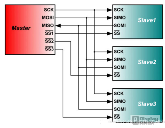
SPI equipment selection
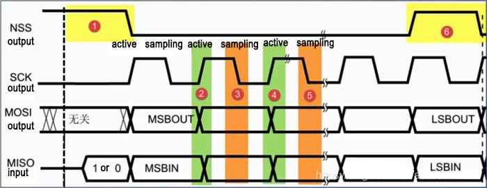
The SPI is a [Single Master Device (single-master)] communication protocol, which means that only one central device in the bus can initiate communication. When the SPI main device wants to read/write [from the device], it first pulls down the corresponding SS line [from the device] (the SS is low-level effective), and then starts to send the working pulse to the clock line. On the corresponding pulse time, [the main device] sends the signal to the MOSI to realize "write", and enables the MISO sampling to realize "read", in the following figure,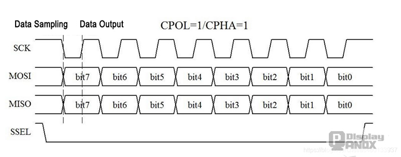
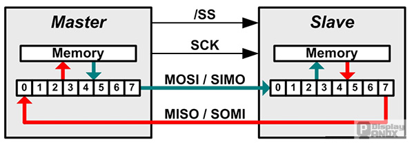
SPI data sending and receiving
Both the SPI host and the slave have a serial shift register, and the host initiates a single transfer by writing a byte to its SPI serial register.1. The corresponding SS signal line is first pulled down to indicate the communication with the device
2. The host tells the slave to write or read the data by sending the SCLK clock signal
Note here that the SCLK clock signal may be either low-level effective or high-level effective because there are four modes of SPI, which we will introduce below
3. The data to be sent by the host (Master) is written to the sending data cache area (Memory), which passes through the shift register (0~7), and the serial shift register moves to the slave byte one by one through the MOSI signal line, and the data received by the MISO interface is moved to the receiving cache area one by one through the shift register.
4. The slave machine (Slave) also returns the contents of its own serial shift register (0~7) to the host via the MISO signal line. Receiving the data sent by the host machine through the MOSI signal line simultaneously, so that the content in the two shift registers is exchanged.
The SPI only has the main mode and the slave mode, and there is no read and write the statement, and the peripheral write operation and read operation is done synchronously. If you write only, the host must only ignore the received bytes; otherwise, if the host wants to read a byte of the slave, it must send an empty byte to trigger the slave transmission. In other words, you send data to receive data; you have to receive data.
Four modes of SPI communication
The four modes of SPI, are simply, set the signal of the SCLK clock signal line as an effective signal.
SPI communication has four different modes of operation, and different slave devices may be configured in some mode at the factory, which cannot be changed; but our communication parties must work in the same mode, so we can configure the SPI mode of our main device through CPOL (Clock Polarity) and CPHA (Clock phase) to control the communication mode of our main equipment, specifically as follows,
Clock polarity (CPOL) defines the clock idle state level,
CPOL=0, indicating that when the SCLK=0 is in an idle state, so the valid state is when the SCLK is at a high level
CPOL=1, indicating that when the SCLK=1 is in an idle state, so the valid state is when the SCLK is at a low level
CPOL=1, indicating that when the SCLK=1 is in an idle state, so the valid state is when the SCLK is at a low level
Clock phase (CPHA) defines the acquisition time of the data,
CPHA=0, sampling the data at the first jump edge (up or down the edge) of the clock., Send data on the second edge
CPHA=1, data sampling at the second jump edge (up or down the edge) of the clock., Send the data at the first edge
CPHA=1, data sampling at the second jump edge (up or down the edge) of the clock., Send the data at the first edge
For instance:
Mode0: CPOL=0, CPHA=0: In the idle state, the SCLK is at the low level, and the data sampling is in the first edge, that is, the SCLK jumps from the low level to the high level, so the data sampling is in the rising edge (prepare data), (send data) data is sent in the descending edge.
Mode1: CPOL=0, CPHA=1: In the idle state, SCLK is at the low level, and data is sent in the first edge, that is, SCLK jumps from the low level to the high level, so data sampling is in the descending edge, and data is sent in the rising edge.
Mode2: CPOL=1, CPHA=0: In the idle state, SCLK is at the high level, and data acquisition is at the first edge, that is, SCLK jumps from high level to low level, so data collection is in the falling edge, and data transmission is sent in the rising edge.
Mode3: CPOL=1, CPHA=1: In the idle state, SCLK is at a high level, data transmission is sent in the first edge, that is, SCLK jumps from high level to low level, so data acquisition is in the rising edge, and data transmission is in the descending edge.
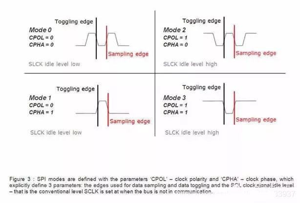
The difference is to define which edge conversion (toggles) output signal of the clock pulse, which edge samples the input signal, and the stable level value of the clock pulse (which is high or low when the clock signal is invalid). Each pattern is characterized by a pair of parameters, called the Clock pole (clock polarity) CPOL and the Clock Period (clock phase) CPHA.
Communication protocol for the SPI
The master-slave device must use the same working mode as —— SCLK, CPOL, and CPHA to work properly. If there are multiple slave devices, and they use different working modes, then the master device must need to modify the mode corresponding to the slave devices when they read and write different slave devices. The main contents of the above SPI bus protocol.
Does it feel like that's all over? So it is with SPI, he does not set the maximum transmission rate, no address scheme, no communication response mechanism, and no flow control rules.
As long as the four signal lines are correctly connected correctly, the SPI mode is the same, the CS / SS signal line down, that is, it can be directly communicated, one byte at a time, read and write data at the same time, this is the SPI
Some communication controls have to be implemented through the SPI devices, and the SPI does not care about the electrical characteristics of the physical interface, such as the standard voltage of the signal.
PS:
This is also a disadvantage of the SPI interface: no specified flow control, and no response mechanism to confirm whether the data is received.
Three modes of the SPI
The SPI works in 3 medium mode, which is run, wait, and stop, respectively.Run Mode
This is the basic mode of operation
Wait Mode
The SPI working-in-waiting mode is a configurable low-power mode that can be controlled by the SPISWAI bit of the SPICR2 register. In waiting mode, if SPISWAI bits 0, the SPI operation is similar to running mode.If SPISWAI position 1, the SPI is in low power consumption, and the SPI clock is off. If the SPI is configured as a host, all transfers stop but restart after the CPU enters running mode. If the SPI is configured as a slave, a byte continues to receive and transmit, ensuring that the slave is synchronized with the host.
Stop Mode
To reduce the power consumption, the SPI is inactive in the stop mode. If the SPI is configured as a host, the ongoing transmission stops, but it resumes after the CPU enters the running mode. If the SPI is configured as a slave, a byte continues to be accepted and sent, ensuring the slave synsynchronized with the host.
SPI Schematic connection
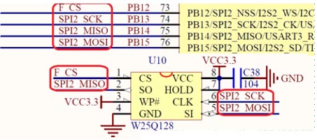
The SPI initialization configuration in STM32
1. Initialize the GPIO port, and configure the multiplexing function of the relevant pins to enable the SPIx clock.Call function: void GPIO_Init ();2. Enabling SPI clock bus: RCC_APB2PeriphClockCmd (RCC_APB2Periph_SPI1, ENABLE)
3. Configure the parameters of the SPI initialization, and set the SPI working mode: SPI_Init (SPI1, & SPI_Initstructure)
4. Enabling SPI peripherals: SPI_Cmd (SPI1, ENABLE);
The SPI configuration settings
typedef struct
{
uint16_t SPI_Direction; /*!<Transmission direction, two-way full-duplex, one-way reception, etc. * /
uint16_t SPI_Mode; /*!<Mode selection to determine the host or slave */
uint16_t SPI_DataSize; /*!<Data size, 8-bit or 16-bit */
uint16_t SPI_CPOL; /*!<Clock polarity selected the */
uint16_t SPI_CPHA; /*!<Clock phase-selected */
uint16_t SPI_NSS; /*!<Select whether the chip is hardware or software * /
uint16_t SPI_BaudRatePrescaler; /*!<Frequency division coefficient: */
uint16_t SPI_FirstBit; /*!<Specifies whether the data transfer starts with an MSB or an LSB bit.M
SB is the binary first, and LSB is the last */
uint16_t SPI_CRCPolynomial; /*!<CRC check, set the CRC check polynomial, improve the pass
Letter reliability, greater than 1 can be * /
}SPI_InitTypeDef;
void SPI2_Init(void)
{
GPIO_InitTypeDef GPIO_InitStructure;
SPI_InitTypeDef SPI_InitStructure;
RCC_APB2PeriphClockCmd( RCC_APB2Periph_GPIOB, ENABLE); / / PORTB clock is enabled
RCC_APB1PeriphClockCmd( RCC_APB1Periph_SPI2, ENABLE); / / SPI2 clock is enabled
GPIO_InitStructure.GPIO_Pin = GPIO_Pin_13 | GPIO_Pin_14 | GPIO_Pin_15;
GPIO_InitStructure.GPIO_Mode = GPIO_Mode_AF_PP; / / PB13 / 14 / 15 Multiplexing push-pull output
GPIO_InitStructure.GPIO_Speed = GPIO_Speed_50MHz;
GPIO_Init (GPIOB, & GPIO_InitStructure); / / Initialize GPIOB
GPIO_SetBits (GPIOB, GPIO_Pin_13 | GPIO_Pin_14 | GPIO_Pin_15); / / PB13 / 14 / 15 pull-up
SPI_InitStructure.SPI_Direction = SPI_Direction_2Lines_FullDuplex; / / Set the SPI one-way or two-way data mode: the SPI is set to double-line two-way full-duplex
SPI_InitStructure.SPI_Mode = SPI_Mode_Master; / / Set the SPI working mode: set the main SPI
SPI_InitStructure.SPI_DataSize = SPI_DataSize_8b; / / Set the data size of SPI: SPI sends 8-bit frame structure
SPI_InitStructure.SPI_CPOL = SPI_CPOL_High; / / The idle status of the serial synchronization clock is a high level
SPI_InitStructure.SPI_CPHA = SPI_CPHA_2Edge; / / The second jump edge (up or down) of the serial synchronization clock is sampled
SPI_InitStructure.SPI_NSS = SPI_NSS_Soft; / / The NSS signal is managed either by either the hardware (NSS pins) or the software (using the SSI bits): the internal NSS signal is controlled by the SSI bits
SPI_InitStructure.SPI_BaudRatePrescaler = SPI_BaudRatePrescaler_256; / / Define the value of wave rate prefrequency: Potter rate prefrequency value is 256
SPI_InitStructure.SPI_FirstBit = SPI_FirstBit_MSB; / / Specifies that data transfer starts from the MSB bit or LSB bit: data transfer starts from the MSB bit
SPI_InitStructure.SPI_CRCPolynomial = 7; / / Polynomial for the CRC values calculated
SPI_Init (SPI2, & SPI_InitStructure); / / Initializes the peripheral SPIx register against the parameters specified in the SPI_InitStruct
SPI_Cmd (SPI2, ENABLE); / / enables SPI peripherals
SPI2_ReadWriteByte (0xff); / / Start the transport
}
SPI Send Function (Standard Library / HAL Library)
Standard library:
u8 SPIx_ReadWriteByte(u8 TxData)
{
u8 retry=0;
while (SPI_I2S_GetFlagStatus(SPI2, SPI_I2S_FLAG_TXE) == RESET)
{
}// waiting send zone is empty
SPI_I2S_SendData (SPI2, TxData); / / Send a byte data via the peripheral SPIx
while (SPI_I2S_GetFlagStatus(SPI2, SPI_I2S_FLAG_RXNE) == RESET)
{
} // waits to receive off a byte
return SPI_I2S_ReceiveData (SPI2); / / Returns data recently received through SPIx
}
HLA storeroom:
uint8_t SPI_SendByte(uint8_t byte)
{
uint8_t d_read,d_send=byte;
if(HAL_SPI_TransmitReceive(&hspi1,&d_send,&d_read,1,0xFFFFFF)!=HAL_OK)
d_read=0XFF;
return d_read;