


This article is a tutorial to drive LCD AT043TN24, the developers can take it as reference.
Related: AT043TN24 LCD parameters
LCD Type
Circuit Connection
Display Principle
TFT LCD Timing
LCD Control Registers
LCD Color Palette
Write The Driver Program
Compilation And Testing
Modify the kernel
Circuit Connection
Display Principle
TFT LCD Timing
LCD Control Registers
LCD Color Palette
Write The Driver Program
Compilation And Testing
Modify the kernel
Development environment
|
Development board
|
JZ2440V3
|
|
CPU
|
SamsunS3C2440
|
|
System
|
Linux3.4.2
|
|
Compiler
|
Arm-linux-gcc 4.3.2
|
|
LCD
|
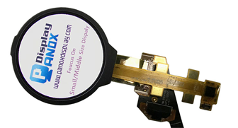
4.3 inch LCD AT043TN24
|
1. LCD type, Circuit connection, Display principle
LCD, or liquid crystal display, is a display that uses transmission technology to control liquid crystal to generate color image. There are many types of LCDS, such as STN, TFT, LTPS, OLED, etc. Each has its advantages and disadvantages.The TFT type LCD above JZ2440V3 development board is also the most mainstream LCD.
There are two data transmission modes for TFT-LCD,
Single Scan: For a whole screen of data, send out one by one, from top to bottom, from left to right.
Double Scan: Divides the whole screen into two parts, and sends the data one by one from top to bottom and from left to right at the same time.
| Signal Name | Description |
| VSYNC | vertical synchronizing signal |
| HSYNC | horizontal synchronizing signal |
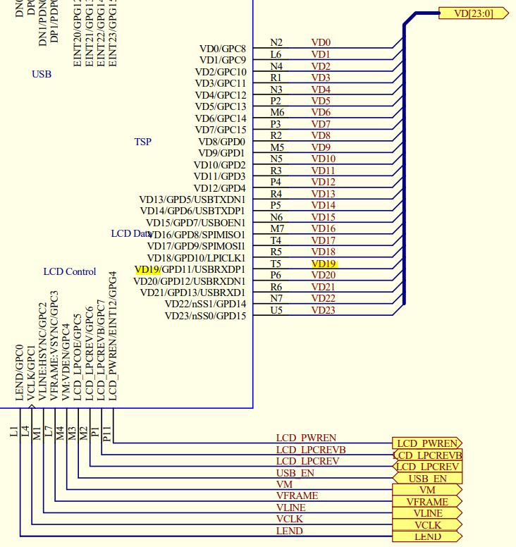
| VD[23:0] | data signal |
| HCLK | Clock signal |
| LEND | Line end signal |
| PWREN | Power switch signal |
Circuit Module
Controller Schematic Diagram
Display Principle
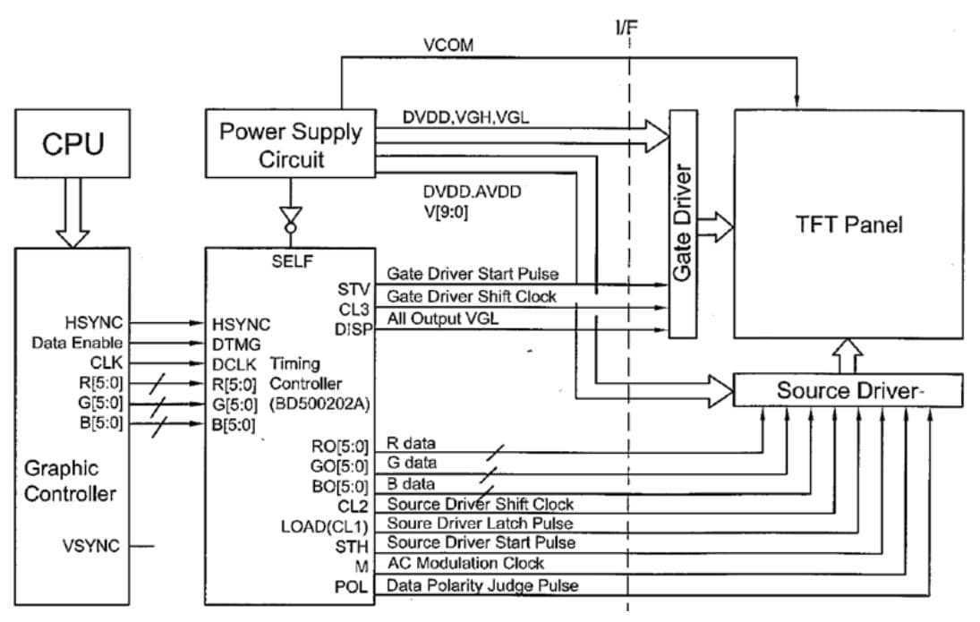
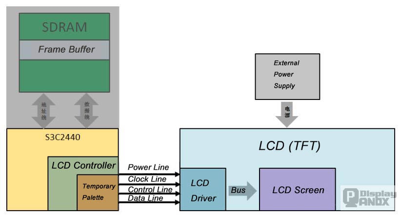
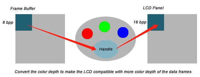
In addition to configuring some registers to tell the LCD controller the format of the pixels in the image (RGB565), the initial address of the frameBuffer, and so on, Some signals are needed to access TFT LCD, so it is necessary to configure registers to tell the LCD controller the information of these signals (such as when to send the control signal, the duration of sending the signal, etc.). For example, When sending picture data to LCD driver, clock control (VCLK) is needed. A clock sends a pixel, then the controller needs to actively send a clock signal, which pin is sent by the clock, and what is the frequency, these are need to be configured. We analyze some signals needed and how to configure them through the sequence diagram. It is difficult to see the sequence directly if you know LCD control for the first time, so just give a visual metaphor first.
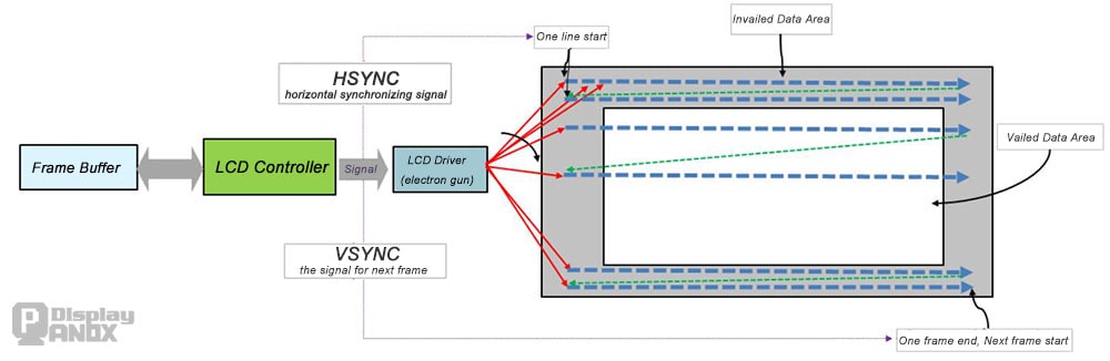
Frame Buffer: The frame buffer is used to store LCD data. frame buffer establishes one-to-one mapping relationship between LCD controller and LCD Panel.
LCD controller: Refer to the LCD user manual to configure the LCD controller, which is used to send LCD control signals and drive the LCD display.
Scanning mode: As shown in the figure, the scanning direction from start to end is: from left to right, from top to bottom (one kind of scanning direction);
HSYNC: Line synchronization signal, which is used for line switching. When a line scan is complete and a new line needs to be scanned, the line synchronization signal needs to be sent first.
VSYNC: Column synchronization signal, used for column switching. When a frame scanning is finished and a new frame needs to be scanned, the column synchronization signal needs to be sent first.
Clock signal: Each time a clock comes, the scanning point shifts one.
In the image above, the LCD driver can be likened to the electron gun, which is controlled by the LCD controller. It takes pixel data from the display cache to the electron gun and sends the command to the electron gun to emit pixel colors
a. The LCD controller sends a VSYNC signal to tell the electron gun that a new frame is coming out, and the electron gun turns the gun to the top left corner of the LCD screen, ready to start firing pixels.
b. At the same time as the VSYNC signal, the HSYNC signal (telling the gun to start a new line, move from left to right to fire the bullet) is issued, but the gun is slow to react and starts firing after a few seconds. For the above two processes, as the electron gun received the VSYNC signal, it would take some time to react before it could work normally after turning the gun head, so several lines of invalid data were shot for nothing, which is equivalent to several HSYNC signal cycles. An HSYNC cycle is the time it takes the gun to sweep a row (the time it takes from the beginning of the HSYNC signal to the end of the first row until the end of the row), and the upper void zone appears.
c. When the first row ends, the LCD controller sends out HSYNC signal again, and the electron gun head twists to the next row and starts transmitting data, but the gun head twists slowly, so there is invalid area left and right (that is, after the end of the first row, the electron gun has to react for some time due to hardware reasons, so there is invalid data area on the right. After turning the gun head, it have to react for a while and start firing bullets, so LCD have this dead zone on the left)Some people will ask how the electron gun knows when the first row is over, actually we tell the LCD controller how many data are in the first row through the register, our screen resolution is 480*272, it will be settled into the regiester.) When a row is over, the LCD controller stops sending valid pixel data and waits for the gun to drift away for a while before sending the HSYNC signal for the next row.
d. Loop c step
e. When the scan reaches the end of the last line (a frame is about to end), the LCD controller will no longer send valid pixel data and wait for the electron gun to drift away for a period of time, so it will continue to scan down and the lower invalid area appears. After that, it will send the VSYNC signal of the next line, and then return to process 1 step and start to repeat.
On a working monitor, you can see a black border around it. The black borer at the top is because, when sending a VSYNC signal, it takes several rows for the first row to be valid; The black border at the bottom is because, when all lines of data are displayed, the display has not scanned to the bottom (the VSYNC signal has not been sent), then the data is invalid; The black border on the left is because when the HSYNC signal is sent, it takes several pixels for the first column of data to be valid; The black border on the right is because when a line of data is displayed, the display has not yet scanned to the far right (HSYNC signal has not been sent), and the data is invalid. The display screen only obtains and displays data according to VSYNC and HSYNC signals, regardless of whether the data is valid. The video card or LCD controller decides when to send valid data.
The frequency at which the VSYNC signal appears indicates how many frames can be displayed in a second. This is called the vertical frequency or field frequency, which is often referred to as the "display frequency". The frequency at which the HSYNC signal appears is called the horizontal frequency, which indicates how many pixels of data can be displayed per second.
On the monitor, the relationship between the storage location of a frame of data and VSYNC and HSYNC signals is shown in the figure below,
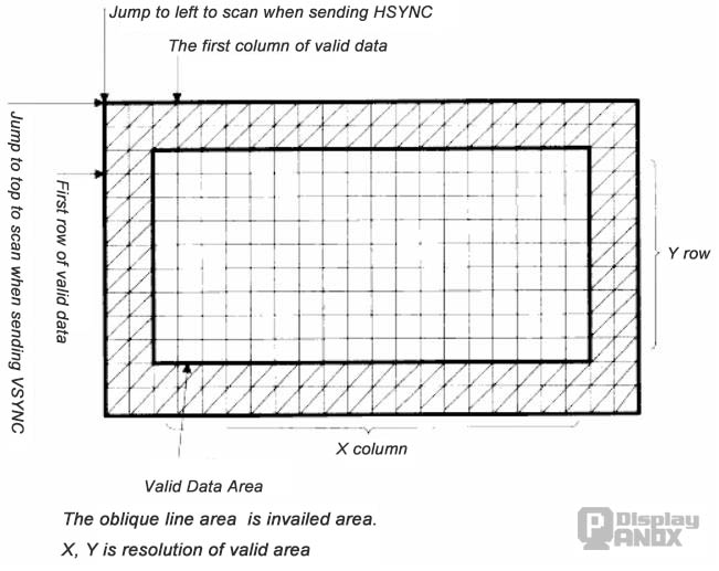
The number of rows and columns of valid data, that is, the resolution, the distance between it and VSYNC, HSYNC signal, etc., can be set, which is completed by the LCD controller.
Data Organization Mode
An image is called a frame. Each frame is composed of multiple lines, each line is composed of multiple pixels, and the color of each pixel is represented by several bits of data. For monochrome displays, each pixel is represented by 1 bit, called 1BPP; For 256-color displays, each pixel is represented by 8 bits, known as 8BPP.
The color of each pixel on the display consists of three parts: Red, Green, and Blue. They are called the three primary colors, and a mixture of the three represents almost all the colors that the human eye can recognize. For example, the three primary colors can be divided into 256 levels according to the depth of the color, then you can use 255 level red, 255 level green, 255 level blue combination into white, or use 0 level red, 0 level green, 0 level blue combination into black.
LCD controller can support monochrome (1BPP), 4-level gray (2BPP), 16-level gray (4BPP), 256 color (8BPP) palette display mode, support 64K(16BPP) and 16M(24BPP) non-palette display mode. The following introduces 64K(16BPP) color display mode, image data storage format.
How Image Store As Data
The 64K(16BPP) color display mode uses 16 bits of data to represent the color of a pixel. The 16-bit data format is divided into two types: 5:6:5 and 5:5:5:1. The 5:6:5 mode uses the front 5 bits to represent red, the middle 6 bits to represent green, and the last 5 bits to represent blue. The 5:5:5:1 mode's front 15 is divided into three five digits from high to low to represent red, green and blue, and the last digit represents transparency. The 5:5:5:1 format is also known as the RGBA format (A:Alpha, for transparency).
A 4-byte data can represent two 16BPP pixels, and it is optional to use the front or last 2 bytes to represent the first pixel. When the display mode is 16BPP, the relationship between memory data and pixel position is as follows,
a.When BSWP=0 and HWSWP=0, the memory pixel arrangement format is as follows,
| Address | D[31:16] | D[15:0] |
| 00H | P1 | P2 |
| 04H | P3 | P4 |
| 08H | P5 | P6 |
| Address | D[31:16] | D[15:0] |
| 00H | P2 | P1 |
| 04H | P4 | P3 |
| 08H | P6 | P5 |
Pixel arrangement on the LCD screen
Mapping between plain color value and VD[23:0] pin
| VD | 23 | 22 | 21 | 20 | 19 | 18 | 17 | 16 | 15 | 14 | 13 | 12 | 11 | 10 | 9 | 8 | 7 | 6 | 5 | 4 | 3 | 2 | 1 | 0 |
| RED | 4 | 3 | 2 | 1 | 0 | NC | NC | NC | NC | NC | NC | NC | NC | |||||||||||
| GREEN | 5 | 4 | 3 | 2 | 1 | 0 | ||||||||||||||||||
| BLUE | 4 | 3 | 2 | 1 | 0 |
The Image Output Mode
a. Display with a frame buffer (most typically)
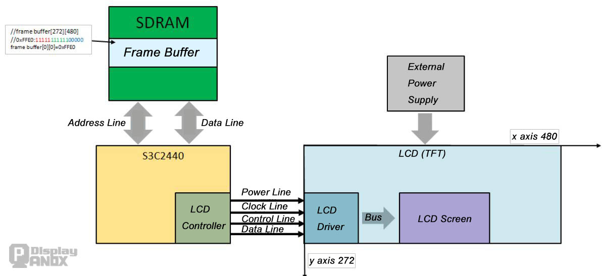
As we see in the figure above, we need to apply for a block of memory in the memory (this memory is called frame buffer), and then configure the LCD controller.
Tell the controller the first address of the frame buffer, and the controller takes the pixel values from the frame buffer and shoots different colors at the LCD screen based on the pixel values. LCD controllers are similar to electron guns,
The LCD controller has a DMA channel inside it. For the frameBuffer, each value corresponds to one pixel of the LCD screen.
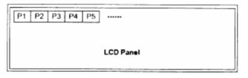
As shown in the figure above, the LCD screen resolution is (480*272). We can define an array with the size of array a[272][480] and tell the LCD controller the address of the array at the beginning.
Then each item of the array corresponds to a pixel of the LCD screen. For example, if a[0][0] is assigned 0xFFE0, the first pixel of the corresponding LCD screen is displayed as yellow.
b. Display Through A Temporary Color Palette
Tips
What Is A Temporary Color Palette
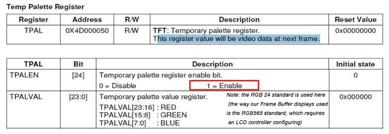
This register value will be video data at next frame. (Tips: One image per frame.)
The temporary color palette is a register, we write the color into this register, then the LCD screen will display the next image is the color recorded in this register, that is, it plays the role of brushing the screen (the whole screen is one color).
When Does It Work And What Does It Do
When this register is enabled, the temporary palette takes effect, and previously configured functions such as display through the frame buffer are invalid, because the LCD screen will be brushed quickly. To achieve this, you do not need to use SDRAM to assign the same value to all elements of the frameBuffer. (tips: With SDRAM, it is already slow). So if you want to restore the previous configuration, disable the Temporary palette function.
What Is A Temporary Color Palette
This register value will be video data at next frame. (Tips: One image per frame.)
The temporary color palette is a register, we write the color into this register, then the LCD screen will display the next image is the color recorded in this register, that is, it plays the role of brushing the screen (the whole screen is one color).
When Does It Work And What Does It Do
When this register is enabled, the temporary palette takes effect, and previously configured functions such as display through the frame buffer are invalid, because the LCD screen will be brushed quickly. To achieve this, you do not need to use SDRAM to assign the same value to all elements of the frameBuffer. (tips: With SDRAM, it is already slow). So if you want to restore the previous configuration, disable the Temporary palette function.
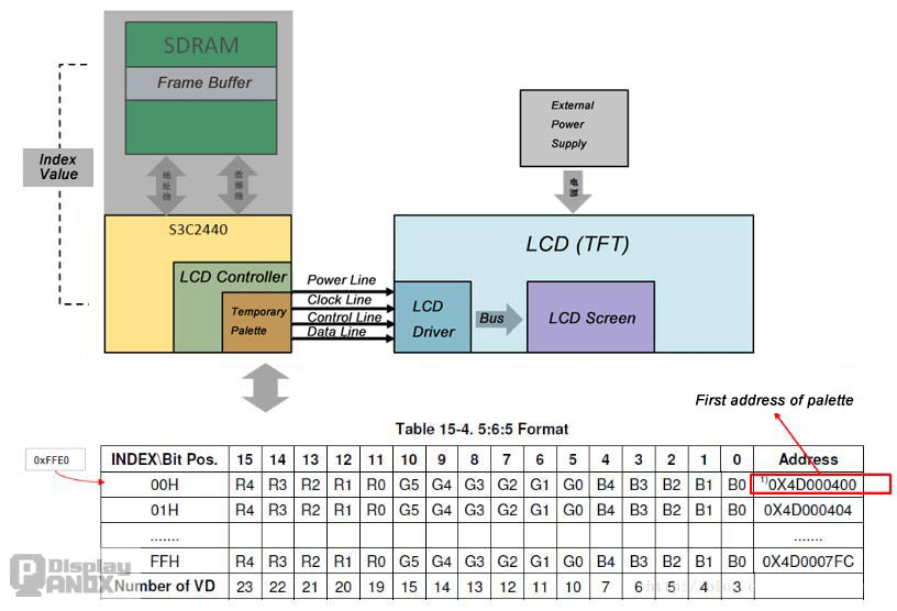
c. Display Through The Color Palette
In the image above, the palette is a block of memory inside the controller (note the difference between the temporary palette). The initial address is 0x4D00400 and there are 256 2-byte sizes (each two bytes represents a color). In the image above, the configuration register tells the LCD controller that the format of the palette is RGB565. The palette then needs to be assigned manually, such as the position in Figure 00H as "yellow". Then, for the framebuffer, each entry represents an index in the palette, such as the first entry of the frameBuffer having a value of 0, The hardware automatically finds the value of the first item in the palette, which is 0xFFE0, and the LCD displays yellow on the first pixel
One more question, how do I enable the color palette? As we mentioned in "Display by frame buffer" above, configuring the register to display 16BPP at 5:6:5 means that the controller assumes that each element in the frame buffer represents a color value and displays it at 5:6:5. But if we set the display mode to 8BPP and the display mode is 5:6:5, the LCD controller automatically assumes that the palette mode is used and the colors in the palette are displayed as (5:6:5). (8Bpp here means that each element in the frame buffer is represented in 8-bit binary notation. The value of each element is the index value in the palette), so what is the application of the palette?
Let` take a 640x480 LCD as example, If the color depth is set to 16 bpp, the picture will appear obvious jitter and incoherence when the system is in use, which is caused by the excessive computing load of the chip. If the palette method mentioned in this paper is adopted, that is, 8-bit color depth display, the selection of colors can meet the needs, and the display of the picture will be obviously stable. This shows that the color palette technology is a very important choice in embedded applications with high display resolution and simple color types.
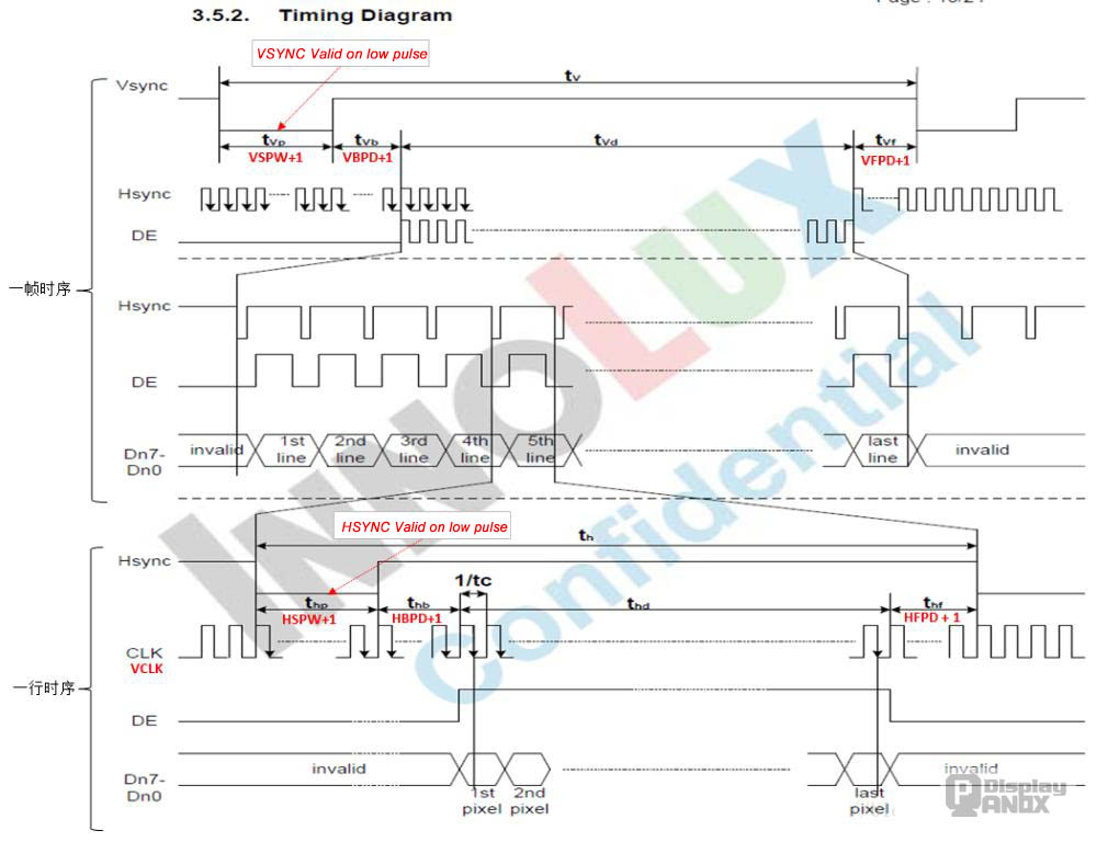
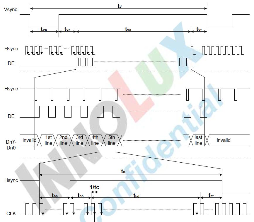
TFT-LCD Timing
Each VSYNC signal represents the beginning of a frame of data; Each HSYNC signal indicates the start of a row of data, whether it is valid or not; Each VCLK signal indicates that one pixel of data is being transmitted, whether it is valid or not. The data is valid only for the CPU's LCD controller, which reads and displays the bus data continuously according to VSYNC, HSYNC, and VCLK.
a. Corresponding to the above process 1,2, the VSYNC signal (representing the beginning of a frame) needs to be sustained for a period of time ②(VSPW+1). The electron gun thinks that the VSYNC signal has been received (i.e. the white strafed VSPW+1 line, It can also be said that the white stringer (VSPW+1) HSYNC cycle time), after receiving the signal, but also continue the duration of ③(VBPD+1), the LCD controller began to send effective data, so that the electron gun emission effective pixels, namely (② + ③) for the LCD screen above the invalid area, for ① parameter, This is the data in the manual, which tells us that the default LCD controller sends HSYNC signal as high level, but the actual LCD accepts HSYNC hardware may be designed as low level effective, so you can modify the register so that the LCD controller sends HSYNC control signal as low level.
Tips: VSPW VBPD parameters are set according to the datasheet (mentioned below), for the purpose of telling the reaction time of the LCD controller to send frame data (for example, after sending HSYNC, sending the valid data after getting the reaction time)
b. ④ is valid data the (LINEVAL + 1) row, and this LCD resolution is 480 * 272, so the LINEVAL is 271 *
c.⑤ VFPD + 1 parameter corresponds to the step 5, when scanning to the end of the last line (i. e., a frame ended), the LCD controller will not send valid pixel data, the electronic gun will stop sending for a period of time, will continue to sweep several lines (VFPD + 1 line) invalid data. LCD controller need to know this time, so that the controller know how long to wait to send VSYNC signal, to start the next frame.
d.For the three parameters, ⑥, ⑦, ⑧, and ⑩, Corresponding to the above-mentioned step 3. After receiving the HSYNC signal (indicating the beginning of a line), this signal must last for a period of ⑦ (HSPW + 1 VCLK cycle), then the electron gun thinks the signal is valid.
After receiving the HSYNC signal, the electron gun also reacts with ⑧ for a period of time (after sweeping HBPD + 1 VCLK cycle, Or, after launching HBPD + 1 invalid pixel), The LCD controller only begins to transmit valid data to the electronic gun, When a line of scan is finished, That is, the LCD controller does not emit valid data, At this point, the electron gun to free for a period of time ⑩ (HFPB + 1), This is time time to tell the LCD controller, To allow the LCD controller to wait to send the HSYNC signal to scan the next line, For the ⑨ parameter, A resolution of 480 * 272, So that HOZVAL = 479, That is, a row has 480 valid data. Note the timing of valid data,after the time (⑦, ⑧), The LCD controller only starts sending valid data.
Parameter Calculation
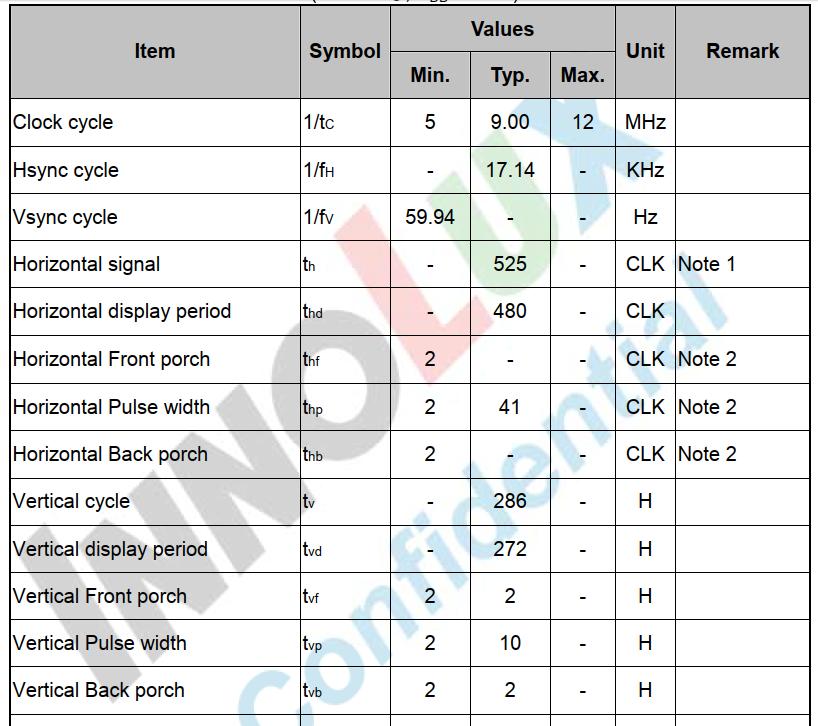
According to the values of the above parameters confirmed by LCD datasheet, the following figure is the timing diagram of the AT043TN24 data manual, and we can easily correspond to the parameters in the timing diagram of the LCD in the 2440 manual above
Tips:
Above figure already marked the corresponding relationship,emphasize a point, VSYNC and HSYNC signal are vaild at low level, but LCD timing is vaild at high level in the 2440 manual, so need to pay attention when configure registers, need to set the two VSYNC, HSYNC signal at low level effective (polarity inversion: default for high level, reverse for low level)
Above figure already marked the corresponding relationship,emphasize a point, VSYNC and HSYNC signal are vaild at low level, but LCD timing is vaild at high level in the 2440 manual, so need to pay attention when configure registers, need to set the two VSYNC, HSYNC signal at low level effective (polarity inversion: default for high level, reverse for low level)
The VSYNC and HSYNC pulse generation depends on the confgurations of both the HOZVAL field and the LINEVAL field in the LCDCON 2/3 registers. The HOZVAL and LINEVAL can be determined by the size of the LCD panel according to the following equations:
--- HOZVAL = (Horizontal display size) -1
--- LINEVAL= (Vertical display size) -1
As we can see, on the left side of the figure above are the specific parameter values, Min, Typ, Max, For example, In the right figure, we know that "VSPW + 1 = tvp", a typical value of tvp in the left figure is 10, in the units of H (Hsync), so VSPW + 1 = 10==> VSPW = 9, The values of the remaining parameters can be determined by the above method, There is also a question left out here, Time of the VSPW, VSPD, VFBD are all dependent on the HSYNC cycle time, so how to confirm the HSYNC cycle time? We can found this sentence in the 2440 manua.
In fact, it means that the LCD controller will confirm the HSYNC time according to the number of pixels emitted by the electronic gun. For example, our LCD screen resolution is 480 * 272. When the VSYNC signal is sent, it will pass the VSPW + 1 reaction time, namely VSPW + 1 HSYNC cycle. We assume that the value of "VSPW + 1" is 10, then it`s 10 HSYNC cycles, that is, after the electronic gun scans 10 x 480 pixels, the LCD controller will experience 10 HSYNC cycle time.
1、VCLK(Hz) = HCLK/[(CLKVAL+1)*2]
2、VSYNC =1/[ {(VSPW+1)+(VBPD+1)+(LIINEVAL+1)+(VFPD+1)} x {(HSPW+1)+(HBPD+1)+(HFPD+1)+(HOZVAL+1)} x {2x (CLKVAL+1) / (HCLK )} ]
3、HSYNC = 1/[{(HSPW+1)+(HBPD+1)+(HFPD+1)+(HOZVAL+1)} x {2x (CLKVAL+1) / (HCLK )}]
After setting the time parameters of VSYNC, HSYNC, VCLK and other signals, and telling the address of the frame memory to the LCD controller, it can automatically issue DMA transmission to get the image data from the frame memory, and finally appear on the data bus VD [23:0] under the control of the above signal. The user only needs to write the image data to the frame memory.
2. LCD Controller REGBANK Register Group
The 17 registers of REGBANK in the LCD controller can be divided into 6 types, as shown in the following table,
For TFT-LCD, only need to set the first two registers, namely LCDCON and LCDSADDR.
| Name | Description |
| LCDCON1~LCDCON5 | Used to select the LCD type and set the time characteristics of various control signals |
| LCDSADDR1~LCDSADDR5 | Address used to set the frame memory |
| TPAL | Temporary color palette register, can quickly output a frame of monochrome image |
| LCDINTPND | For LCD interruption,not necessarily in general applications |
| LCDSRCPND | For LCD interruption,not necessarily in general applications |
| LCDINTMSK | For LCD interruption,not necessarily in general applications |
| REDLUT | Dedicated for STN-LCD |
| GREENLUT | Dedicated for STN-LCD |
| BLUELUT | Dedicated for STN-LCD |
| DITHMODE | Dedicated for STN-LCD |
| TCONSEL | Dedicated for SEC TFT-LCD |
2.1 The LCD Control Register LCDCON1
It is mainly used to select the LCD type, setting the pixel clock, enabling the output of the LCD signal, etc. The format is shown in the following table,
| LCDCON1 | Bit | Description |
| LINECNT | [27:18] | Provide the status of the line counter Read-only, count from LINEVAL to 0 |
| CLKVAL | [17:8] | Determine the rates of VCLK (pixel clock) and CLKVAL[9:0] |
| MMODE | [7] | Detemine the toggle rate of VM signal for STN-LCD |
| PNRMODE | [6:5] | Select the display mode, set 0b11 for TFT-LCD |
| BPPMODE | [4:1] | Select the BPP, for TFT-LCD: 0 b1100 = 16 BPP |
| ENVID | [0] | LCD video output enable bits, 0-prohibit, 1-enable |
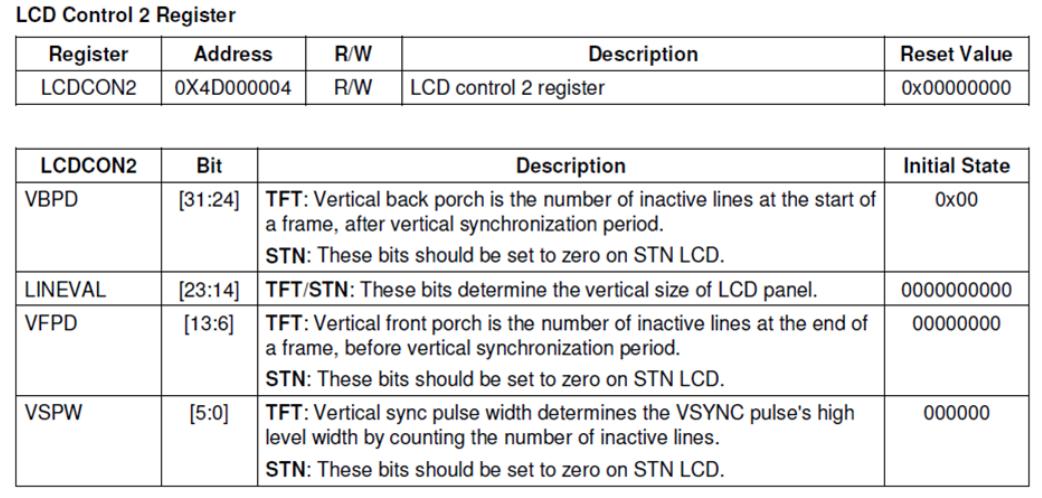
2.2 The LCD Control Register LCDCON2
Time parameters is for setting each signal in the vertical direction, the format is shown in the following table,
| LCDCON2 | Bit | Description |
| VBPD | [31:24] | After VSYNC signal pulse, and after (VBPD + 1) HSYNC signal cycle, valid row data appears; |
| LINEVAL | [23:14] | Vertical width of the LCD, (LINEVAL + 1) row; |
| VFPD | [13:6] | Number of invalid rows up to the next VSYNC signal after the valid data in one frame: VFPD + 1 line; |
| VSPW | [5:0] | For the pulse width bit (VSPW + 1) of the HSYNC signal period, representing the (VSPW + 1) line, the data for this (VSPW + 1) line is invalid |
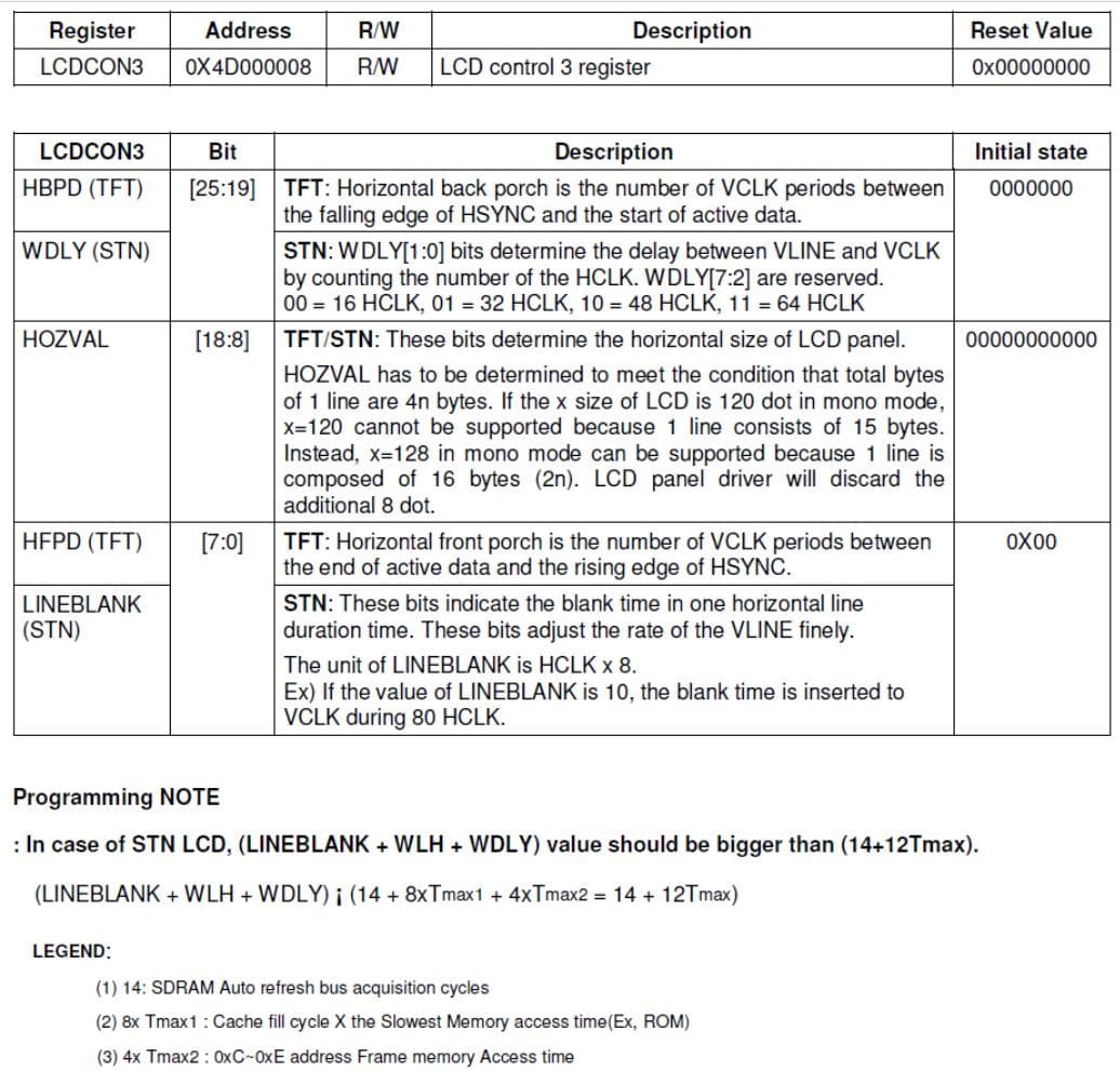
2.3 The LCD Control Register LCDCON3
It`s used to settle time parameters for each signal in the horizontal direction in the format shown in the following figure,
| LCDCON3 | Bit | Description |
| HBPD | [25:19] | After the HSYNC signal pulse, another (HBPD + 1) VCLK signal cycle is passed before the effective pixel data appears |
| HOZVAL | [18:8] | Horizontal width of the LCD, (HOZVAL + 1) class (pixels); |
| HFPD | [7:0] | After the end of the valid data in one row, the number of invalid pixels before the next HSYNC signal is valid, HFPD + 1 pixel; |
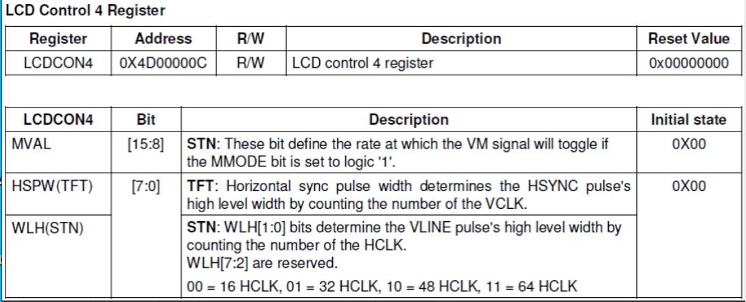
2.4 The LCD Control Register LCDCON4
For TFT-LCD, this register is only used to set the pulse width of the HSYNC signal, the value [7:0] is called HSPW, representing the pulse width bit (HSPW + 1) VCLK period.
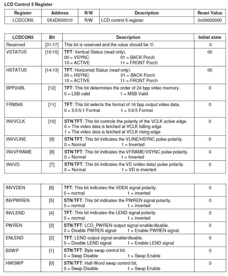
2.5 The LCD Control Register LCDCON5
It`s to set the polarity of each control signal and reads some status information in the format shown in the following table,
| LCDCON5 | Bit | Description |
| VSTATUS | [16:15] | Read-only, vertical; 00: during the pulse of the VSYNC signal; 01: between the end of the VSYNC signal and the valid line; 10: in the valid line; 11: between the valid end of the line and the next VSYNC signal; |
| HSTATUS | [14:13] | Read-only, horizontal state; 00: during the HSYNC signal pulse; 01: between the HSYNC signal end and the pixel active; 01: in the pixel active; 11: between the pixel active end and the next HSYNC signal; |
| BPP24BL | [12] | When the display mode of TFT-LCD is 24 BPP, which 3 bytes of a 4 bytes are valid, 0: LSB is valid, 1: MSB is valid (3 bytes of high address); |
| FRM565 | [11] | The data format used when the display mode of TFT-LCD is set to 16 BPP, 0 means 5:5:5:1 format, 1 means 5:6:5 format; |
| INVVCLK | [10] | Setting the VCLK signal effective along polarity: 0 represents the read data along the VCLK; 1 represents the read data along the VCLK; |
| INVVLINE | [9] | Set the polarity of the VINE / HSYNC pulse; 0 indicates the normal polarity, and 1 represents the reversal polarity; |
| INVVFRAME | [8] | Set the polarity of the VFRAME / VSYNC pulse; 0 = the normal polarity, 1 = the inversion polarity; |
| INVVD | [7] | Set VD data line represents the polarity of data; 0 = normal polarity, 1 = inversion polarity; |
| INVVDEN | [6] | Set the polarity of VDEN signal; 0 = the normal operation, 1 = the polarity of inversion; |
| INVPWREN | [5] | Set the polarity of PWREN signal; 0 = the normal operation, 1 = the polarity of inversion; |
| INVLEND | [4] | Set the polarity of LEND signal; 0 = the normal operation, 1 = the polarity of inversion; |
| PWREN | [3] | LCD _ PWREN signal output enable; 0 = Swap Disable,1 = Swap Enable |
| ENLEND | [2] | LEND signal output enable; 0 = Swap Disable,1 = Swap Enable |
| BSWP | [1] | Byte exchange enabling; 0 = Swap Disable,1 = Swap Enable |
| HWSWP | [0] | Half Byte (2 bytes) exchange enabling; 0 = Swap Disable,1 = Swap Enable |
2.6 Frame Memory Address Register LCDSDRR1~LCDSDRR3
The frame memory can be large, and the real area to be displayed is called the "viewport" , which is within the frame memory. These three registers are used to determine the starting address of the frame memory and locate the position of the viewport in the frame memory.
The following figure shows the positional relationship between the frame memory and the viewports,
The following figure introduces each frame memory register,
LCDSADRR1 register format
| LCDSADRR1 | Bit | Description |
| LCDBANK | [29:21] | Used to save the frame memory start address A [30:22], the frame memory start address must be 4MB aligned |
| LCDBASEU | [20:0] | For TFT-LCD, save the memory start address corresponding to the viewport A [21:1], which is also called the frame buffer (frame buffer) for LCD; |
LCDSADRR2 register format
| LCDSADRR2 | Bit | Description |
| LCDBASEL | [20:0] | For TFT-LCD, the frame buffer end address used to save the LCD A [21:1], the value can be calculated as follows: LCDBASEL=LCDBASEU + (PAGEWIDTH + OFFSIZE) * (LINEVAL + 1) |
Note: The values of LCDBASEU and LCDBASEL can be modified to move the image, but it cannot be modified at the end of a frame image.
LCDSADRR3 register format
| LCDSADRR3 | Bit | Description |
| OFFSIZE | [21:11] | It represents the half byte of the address difference between the last data of the previous row and the first data of the next row, that is, the address difference in half digits; 0 means that two lines of data are followed, 1 means two bytes between them, and so on. |
| PAGEWIDTH | [10:0] | Width of the viewport in half digits. |
3. Color Palette
Temporary Color Palette Register TPAL
If you want to output a monochrome image, you can set this color value in the TPL register and then enable the TPAL register, which can avoid modifying the entire palette or frame buffer.
TPAL Register Format
| Register | Bit | Description |
| TPALEN | [24] | Palette register enable vibits, 0=Disable,1=Enable |
| TPALVAL | [23:0] | Color value; TPALVAL [23:16]: Red TPALVAL [15:8]: Green TPALVAL [7:0]: blue |
Note: The temporary palette register TPAL can be used in any display mode, not only in the 8 BPP mode
4. Write The Driver Program
4.1 LCD.C
Build the Overall Framework
Referring to the associated lcd driver (drivers / video /), add the header file,
#include <linux/module.h>
#include <linux/kernel.h>
#include <linux/errno.h>
#include <linux/err.h>
#include <linux/string.h>
#include <linux/mm.h>
#include <linux/slab.h>
#include <linux/delay.h>
#include <linux/fb.h>
#include <linux/init.h>
#include <linux/dma-mapping.h>
#include <linux/interrupt.h>
#include <linux/workqueue.h>
#include <linux/wait.h>
#include <linux/platform_device.h>
#include <linux/clk.h>
#include <linux/cpufreq.h>
#include <asm/io.h>
#include <asm/uaccess.h>
#include <asm/div64.h>
#include <asm/mach/map.h>
#include <mach/regs-lcd.h>
#include <mach/regs-gpio.h>
#include <mach/fb.h>
static struct fb_info *s3c_lcd;
static int lcd_init(void)
{
/* 1. Assign one fb_info */
s3c_lcd = framebuffer_alloc(0, NULL);
/* 2. Config */
/* 2.1 Set Fixed Parameters */
/* 2.2 Set Variable parameters */
/* 2.3 Set the operation function */
/* 2.4 Setting other contents */
/* 3. Hardware related operations */
/* 3.1 Configuring GPIO for LCD */
/* 3.2 Set the LCD controller according to the LCD manual, such as the VCLK frequency */
/* 3.3 Allocate video memory (frambuffer) and tell the address to the LCD controller */
/* 4. Register */
register_framebuffer(s3c_lcd);
return 0;
}
static void lcd_exit(void)
{
}
module_init(lcd_init);
module_exit(lcd_exit);
MODULE_LICENSE("GPL");
The entry function lcd_init()
Assign an fb_info
s3c_lcd = framebuffer_alloc(0, NULL);
Set the fixed parameter —— fb_fix_screeninfo structure
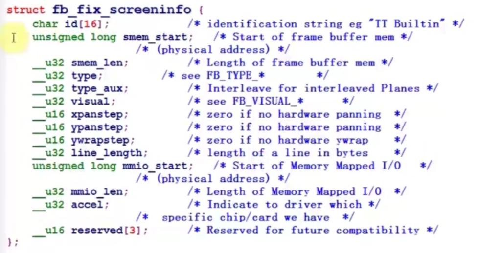
/* 2.1 Set fixed parameters */strcpy(s3c_lcd->fix.id, "mylcd");
s3c_lcd->fix.smem_len = 480*272*16/8; //Screen resolution 480X272, 16bpp/pix
s3c_lcd->fix.type = FB_TYPE_PACKED_PIXELS; //Screen type
s3c_lcd->fix.visual = FB_VISUAL_TRUECOLOR; /* True Color TFT */
s3c_lcd->fix.line_length = 480*2; //Line required storage length =480 pixels X2 bytes
s3c_lcd->fix.smem_len = 480*272*16/8; //Screen resolution 480X272, 16bpp/pix
s3c_lcd->fix.type = FB_TYPE_PACKED_PIXELS; //Screen type
s3c_lcd->fix.visual = FB_VISUAL_TRUECOLOR; /* True Color TFT */
s3c_lcd->fix.line_length = 480*2; //Line required storage length =480 pixels X2 bytes
Set Variable Parameters
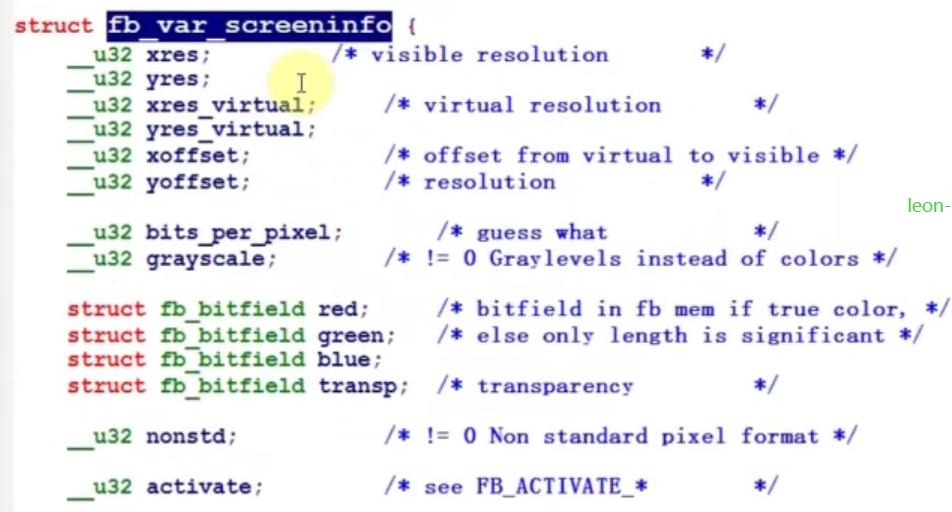
/* 2.2 Set variable parameters */
s3c_lcd->var.xres = 480; //Resolution in the X direction
s3c_lcd->var.yres = 272; //Resolution in the y direction
s3c_lcd->var.xres_virtual = 480; //X direction virtual resolution
s3c_lcd->var.yres_virtual = 272; //Virtual resolution in the y direction
s3c_lcd->var.bits_per_pixel = 16; //How many bits are in each pixel
/* RGB:565 */
s3c_lcd->var.red.offset = 11; //Starting at number 11
s3c_lcd->var.red.length = 5; //It's 5 places
s3c_lcd->var.red.msb_right = 0; //Is the data to the right of offset? The default value is 0, indicating the left side (high direction). You don't need to set it
s3c_lcd->var.green.offset = 5; //Start at number five
s3c_lcd->var.green.length = 6;
s3c_lcd->var.blue.offset = 0; //Let's start with the 0 digit
s3c_lcd->var.blue.length = 5;
s3c_lcd->var.activate = FB_ACTIVATE_NOW; //Use the default values for now
Set The Operation Function —— fbops
s3c_lcd->fbops = &s3c_lcdfb_ops;
Define fb_ops structure outside the function,
static struct fb_ops s3c_lcdfb_ops = {
.owner = THIS_MODULE,
.fb_setcolreg = s3c_lcdfb_setcolreg, //Palette setting function
.fb_fillrect = cfb_fillrect,
.fb_copyarea = cfb_copyarea,
.fb_imageblit = cfb_imageblit,
};
.owner = THIS_MODULE,
.fb_setcolreg = s3c_lcdfb_setcolreg, //Palette setting function
.fb_fillrect = cfb_fillrect,
.fb_copyarea = cfb_copyarea,
.fb_imageblit = cfb_imageblit,
};
Other Setting
s3c_lcd->pseudo_palette = pseudo_palette; //Palette array address
s3c_lcd->screen_base = ; /* The virtual address of video memory */
s3c_lcd->screen_size = 480*272*16/8;
s3c_lcd->screen_base = ; /* The virtual address of video memory */
s3c_lcd->screen_size = 480*272*16/8;
Hardware-Related Operations
Configure the GPIO for the LCD
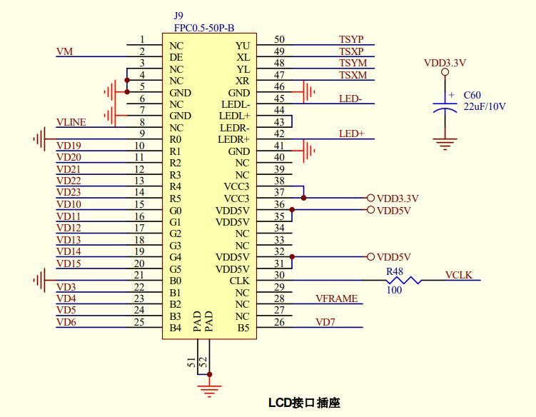
LCD Interface socket
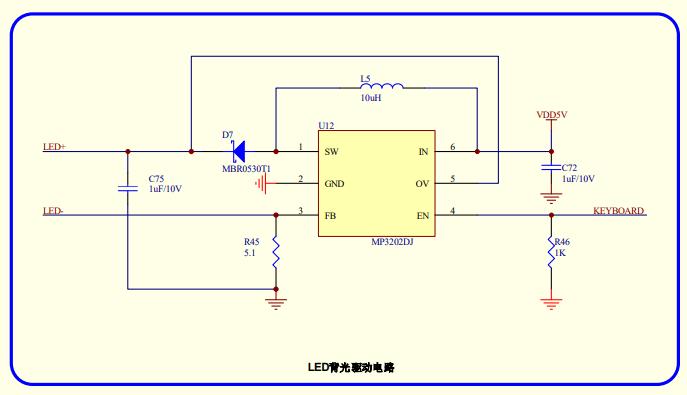
LED backlight driver circuit
According to the schematic diagram, all the used pins are to be configured. Then view the schematic diagram and find the IO port corresponding to each pin,
LED backlight driver circuit
According to the schematic diagram, all the used pins are to be configured. Then view the schematic diagram and find the IO port corresponding to each pin,
First, define the register pointer variable for the IO port outside the function,
tatic volatile unsigned long *gpbcon;static volatile unsigned long *gpbdat;static volatile unsigned long *gpccon;static volatile unsigned long *gpdcon;static volatile unsigned long *gpgcon;
Then map the address within the function,
/*Configure GPIO for LCD*/// / Even if you write only 4 bytes, the system will still map at least 1 page (4KB)
gpbcon = ioremap(0x56000010, 8);
gpbdat = gpbcon+1;
gpccon = ioremap(0x56000020, 4);
gpdcon = ioremap(0x56000030, 4);
gpgcon = ioremap(0x56000060, 4);
*gpccon = 0xaaaaaaaa; /* GPIO pin for VD[7:0],LCDVF[2:0],VM,VFRAME,VLINE,VCLK,LEND */*gpdcon = 0xaaaaaaaa; /* GPIO pin forVD[23:8] */
/* GPB0 Set as output pin */*gpbcon &= ~(3); *gpbcon |= 1;*gpbdat &= ~1; /* First output low level to turn off the backlight power supply */
*gpgcon |= (3<<8); /* GPG4用作LCD_PWREN(LCD power) */
Set the LCD controller, such as the VCLK frequency, according to the LCD manual
First, check the S3C2440 chip manual and set the control registers in the LCD controller chapter. To facilitate the reference, we first define a global structure (lcd_regs), which is the address of each register.approach,
struct lcd_regs {
unsigned long lcdcon1;
unsigned long lcdcon2;
unsigned long lcdcon3;
unsigned long lcdcon4;
unsigned long lcdcon5;
unsigned long lcdsaddr1;
unsigned long lcdsaddr2;
unsigned long lcdsaddr3;
unsigned long redlut;
unsigned long greenlut;
unsigned long bluelut;
unsigned long reserved[9];
unsigned long dithmode;
unsigned long tpal;
unsigned long lcdintpnd;
unsigned long lcdsrcpnd;
unsigned long lcdintmsk;
unsigned long lpcsel;
};
Then, define a pointer to a structure of that type, 'lcd_regs' :
static volatile struct lcd_regs* lcd_regs; // All addresses to registers must be volatile
Finally, perform the address mapping in the 'lcd.c' function, and then set the LCD control register according to the LCD data manual,
LCD Time Paremeters
LCD Time Series
lcd_regs = ioremap(0x4D000000, sizeof(struct lcd_regs));
//1.Set the LCDCON1 register
/* CLKVAL => bit[17:8]: VCLK = HCLK / [(CLKVAL+1) x 2],
* VCLK Get the value by checking the Clock cycle in Section 3.5.1 of the LCD manual
* 9MHz(Typ) = 100MHz / [(CLKVAL+1) x 2]
* CLKVAL = 4(Let's take the integer 4 here)
* MMODE => bit[7]:Take the default
* PRNMODE => bit[6:5]: 0b11 (TFT LCD panel)
* BPPmode => bit[4:1]: 0b1100(16 bpp for TFT)
* ENVID => bit[0] : 0b0 (Disable it temporarily, turn it on when you need to.)
*/
lcd_regs->lcdcon1 = (4<<8) | (3<<5) | (0x0c<<1);
//2.Set the LCDCON2-4 register
#if 1
/* Time parameter in the vertical direction
* VBPD => bit[31:24]: 1, CHow long will it take for row 1 to be emitted after VSYN
* LINEVAL => bit[23:14]: 271, so LINEVAL=272-1=271
* VFPD => bit[13:6] : 1, How long does it take to send VSYNC after the last row, so VFPD=2-1=1
* VSPW => bit[5:0] : 9, Pulse width of VSYNC signal,VSPW=10-1=9
*/
lcd_regs->lcdcon2 = (1<<24) | (271<<14) | (1<<6) | (9);
/* Horizontal time parameter
* HBPD => bit[25:19]: 1, How long does it take to send the first line after VSYNC? HBPD=2-1
* HOZVAL => bit[18:8]: 479, HOZVAL=480-1=479
* HFPD => bit[7:0] : 1 , How long does it take to issue HSYNC after sending the last pixel in the last row,HFPD=2-1=1
*/
lcd_regs->lcdcon3 = (1<<19) | (479<<8) | (1);
/* Horizontal synchronization signal
* HSPW => bit[7:0]: 40, Pulse width of HSYNC signal, HSPW=41-1=40
*/
lcd_regs->lcdcon4 = 40;
#else
lcd_regs->lcdcon2 = S3C2410_LCDCON2_VBPD(5) |
S3C2410_LCDCON2_LINEVAL(319) |
S3C2410_LCDCON2_VFPD(3) |
S3C2410_LCDCON2_VSPW(1);
lcd_regs->lcdcon3 = S3C2410_LCDCON3_HBPD(10) |
S3C2410_LCDCON3_HOZVAL(239) |
S3C2410_LCDCON3_HFPD(1);
lcd_regs->lcdcon4 = S3C2410_LCDCON4_MVAL(13) |
S3C2410_LCDCON4_HSPW(0);
#endif
/* Polarity of signal
* bit[11]: 1=565 format
* bit[10]: 0 = According to the LCD manual, it takes data at the falling edge
* bit[9] : 1 = HSYNC signal to be reversed (compare the timing diagram of S3C2440 manual and LCD manual)
* bit[8] : 1 = VSYNC signal to reverse,
* bit[7] : 0 = INVVD no inversion (low data pin indicates data 1)
* bit[6] : 0 = VDEN without inversion (compare the sequence diagram of S3C2440 manual and LCD manual)
* bit[5] : 0 = INVPWREN no inversion (power enable switch high level active)
* bit[3] : 0 = PWREN signal output enable (temporarily do not enable it, and then open it after setting)
* bit[1:0] : 01,memory data and pixel correspondence, 00 represents D[31:0] high 8 bits correspond to Pix1,
* The low 8 bits correspond to Pix2,01 indicates the high 8 bits of D[31:0] correspond to Pix2, and the low 8 bits correspond to Pix1
* S3C2440 Manual page 413
*/
lcd_regs->lcdcon5 = (1<<11) | (0<<10) | (1<<9) | (1<<8) | (1<<0);
Alsign video memory (frambuffer) and address the LCD controller and finally start the LCD
/* screen_base: virtual address of video memory; smem_start: indicates the physical address of video memory.*/
s3c_lcd->screen_base = dma_alloc_writecombine(NULL, s3c_lcd->fix.smem_len, &s3c_lcd->fix.smem_start, GFP_KERNEL);
/* The starting address of the Frame Buffer
* LCDBANK => bit[29:21]: ,corresponds to the A[30:22] bit of the start address of the video cache (4MB address alignment)
* LCDBASEU => bit[20:0]: ,corresponds to the A[21:1] bit of the start address of the video cache,
*/
lcd_regs->lcdsaddr1 = (s3c_lcd->fix.smem_start >> 1) & ~(3<<30);
/* End address of the Frame Buffer
* LCDBASEL => bit[20:0]: ,orresponds to the A[21:1] bit of the end address of the video cache,
*/
lcd_regs->lcdsaddr2 = ((s3c_lcd->fix.smem_start + s3c_lcd->fix.smem_len) >> 1) & 0x1fffff;
/* The width of the effective display area of the Frame Buffer (in half a word, in 2 bytes)
* OFFSIZE => bit[21:11]: ,use the default value
* PAGEWIDTH => bit[10:0]: ,the length of a line (unit: 2 bytes)
*/
lcd_regs->lcdsaddr3 = (480*16/16);
/* Start LCD*/
lcd_regs->lcdcon1 |= (1<<0);/* Indicates that the ENVID signal is enabled, indicating data transmission */
lcd_regs->lcdcon5 |= (1<<3); /* Enable the PWREN signal */
*gpbdat |= 1; /* Output high level, enable backlight */
Register
/* 4. register */
register_framebuffer(s3c_lcd);
register_framebuffer(s3c_lcd);
Output Function lcd_exit()
static void lcd_exit(void)
{
unregister_framebuffer(s3c_lcd); //Log out of fb
lcd_regs->lcdcon1 &= ~(1<<0); /* Stops sending data to the LCD */
lcd_regs->lcdcon5 &= ~(1<<3); /* Turn off PWREN signal */
*gpbdat &= ~1; /* Turn off the backlight */
//dma_free_writecombine(device, memory length, virtual start address, start physical address)
dma_free_writecombine(NULL, s3c_lcd->fix.smem_len, s3c_lcd->screen_base, s3c_lcd->fix.smem_start);
iounmap(lcd_regs);
iounmap(gpbcon);
iounmap(gpccon);
iounmap(gpdcon);
iounmap(gpgcon);
framebuffer_release(s3c_lcd); //Release fb
}
Palette Function Setting
For compatibility, we should define a pseudo-palette array first,
static u32 pseudo_palette[16];
Set the color fill function
/* from pxafb.c */static inline unsigned int chan_to_field(unsigned int chan, struct fb_bitfield *bf)
{
chan &= 0xffff;
chan >>= 16 - bf->length;
return chan << bf->offset;
}
{
chan &= 0xffff;
chan >>= 16 - bf->length;
return chan << bf->offset;
}
Set the palette
static int s3c_lcdfb_setcolreg(unsigned int regno, unsigned int red,
unsigned int green, unsigned int blue,
unsigned int transp, struct fb_info *info)
{
unsigned int val;
if (regno > 16)
return 1;
/* 用red,green,blue the three primary colors form val */
val = chan_to_field(red, &info->var.red);
val |= chan_to_field(green, &info->var.green);
val |= chan_to_field(blue, &info->var.blue);
//((u32 *)(info->pseudo_palette))[regno] = val;
pseudo_palette[regno] = val;
return 0;
}
Overall Code Structure of LCD.C file
It`s a little long, just download the LCD.C file here
lcd.c
5. Compilation And Testing
Open the graphical configuration interface for the kernel
cd ~/linux3.4.2/
make menuconfig
make menuconfig
Modularity kernel`s LCD driver
Enter Device Drivers——>Graphics support——>Support for frame buffer devices, Remove the check off, Select the Modular [S3C2410 LCD framebuffer support] option (because the three functions cfb _ fillrect, cfb _ copyarea, cfb _ imageblit are needed in the fops of our driver, And they are located in the module of the kernel).
Recompile the kernel and install the module
cd ~/linux3.4.2
make uImage
make modules
cd arch/arm/boot
mv uImage uImage_nolcd
cd ~/linux3.4.2
//Copy the new kernel to the tftp shared folder
cp arch/arm/boot/uImage_nolcd /mnt/hghf/virtual_shared/tftp
//Copy the driver module cfb*.ko containing cfb_fillrect, cfb_copyarea, and cfb_imageblit to the network file system
cp drivers/video/cfb*.ko ~/nfs_root/first_fs
Start the development board with the new kernel
// When starting the development board, press any key to access the uboot menu
# q // Exit the menu and go to the command line
// Copy the newly compiled kernel to the tftp shared folder and then execute the following statement
# tftp 30000000 uImage_nolcd ec// Download the kernel image to 30000000 memory
// or use the NFS service to download the file to 300 million places in the memory
# NFS 30000000 192.168.1.101: / home/Leon/nfs_root/first_fs/uImage
# bootm 30000000 // Boot
// After the system is successfully started, mount the network file system
# mount NFS - o nolock 192.168.1.101: / home/Leon/nfs_root first_fs/MNT
Install the driver module, cfb *. The ko and lcd driver
Switch back to the developer board serial port terminal and execute the following command,
//Install the three copied modules
# insmod cfbcopyarea.ko
# insmod cfbfillrect.ko
# insmod cfbimgblt.ko
//Install the LCD driver
# insmod lcd.ko
//Check whether the installation is successful
# ls /dev/fb*
/dev/fb0 //The newly installed fb0 appears in the device file, and the development board screen lights up
# insmod cfbcopyarea.ko
# insmod cfbfillrect.ko
# insmod cfbimgblt.ko
//Install the LCD driver
# insmod lcd.ko
//Check whether the installation is successful
# ls /dev/fb*
/dev/fb0 //The newly installed fb0 appears in the device file, and the development board screen lights up
3 ways to test LCD driver
write any data to driver file, to see whether LCD screen has messy pictures
# cat anyfile > /dev/fb0
Or output the string to the screen to see if the LCD screen has the string output
# echo "hello darkbird!" > /dev/tty1
Modify /etc/inittab file, add tty1, restart the new kernel, reinstall each module before test
tty1: Input corresponds to the development board keyboard, output corresponds to our LCD, and the corresponding driver file is the previously written buttons.ko
tty1::askfirst:-/bin/sh
# mount -nfs -o nolock 192.168.1.101:/home/leon/nfs_root/first_fs /mnt
# cd /mnt
# insmod cfbcopyarea.ko
# insmod cfbfillrect.ko
# insmod cfbimgblt.ko
# insmod lcd.ko
# insmod buttons.ko
Then press the button on the development board, the LCD frequency screen will enter the command line,
After that, press the three keys corresponding to ls + return, and display the ` ls ` command execution result on the screen.
6. Modify the kernel comes with an lcd drive to support a 4.3-inch (480X272) screen
6.1 Analysis and modification of the linux kernel driver framework
The lcd display uses the standard frame buffer subsystem in the linux kernel. Frame buffer (FrameBuffer) is an interface provided by Linux for display devices, Users can view the frame buffer as an image of the display memory, After mapping it to the process address space, You can read and write directly, And the writing operation can be immediately reflected on the screen, This operation is both abstract and unified, Users do not have to care about the location of the video memory, the page change mechanism and other specific details, These are all driven by FrameBuffer devices, Frame buffer describes the display device as a buffer, Allow applications to access these graphics devices through defined interfaces with a frame buffer, So you don't have to care about the specific hardware details.
The LCD driver using the frame buffer subsystem involves three files:
fbmem.c: The specific details of frame buffer is just an abstract layer, providing the operation function interface and the hardware operation function.
s3c2410fb.c: For initializing an lcd hardware device, containing specific details of the hardware operation.
mach-smdk2440.c: Provides the configuration information of LCD display, such as length, width, pixel number, pixel clock frequency, and the timing of LCD display.
6.2 Modify the mach-smdk2440.c code
(the LCD driver part)
/* LCD driver info */
/************************************************************************/
static struct s3c2410fb_display smdk2440_lcd_cfg __initdata = {
.lcdcon5 = S3C2410_LCDCON5_FRM565 |
S3C2410_LCDCON5_INVVLINE |
S3C2410_LCDCON5_INVVFRAME |
S3C2410_LCDCON5_PWREN |
S3C2410_LCDCON5_HWSWP,
.type = S3C2410_LCDCON1_TFT,
.width = 480,
.height = 272,
.pixclock = 111000,
.xres = 480,
.yres = 272,
.bpp = 16,
.left_margin = 2,/*HBP=VBPD+1,line switch, delay between synchronization and drawing*/
.right_margin = 2,/*HFP=HFPD+1,line switch, delay between drawing and synchronization*/
.hsync_len = 41,/*HSPW+1, horizontal synchronization length */
.upper_margin = 2, /*VVBP=VBPD+1, frame switch, delay between synchronization and drawing */
.lower_margin = 2, /*VFB=VFPD+1,frame switch, delay between drawing and synchronization*/
.vsync_len = 10,/*VSPW+1,the length of vertical synchronization*/
};
static struct s3c2410fb_mach_info smdk2440_fb_info __initdata = {
.displays = &smdk2440_lcd_cfg,
.num_displays = 1,
.default_display = 0,
#if 1
/* currently setup by downloader */
.gpccon = 0xaaaaaaaa, /* Configure the GPC port as LCD control pin */
.gpccon_mask = 0xffffffff,
.gpcup = 0xffff, /* banned GPC port internal pull-up */
.gpcup_mask = 0x0000,
.gpdcon = 0xaaaaaaaa, /* Configure the GPD port as LCD control pin */
.gpdcon_mask = 0xffffffff,
.gpdup = 0xffff, /* no pulling GDP port on internal */
.gpdup_mask = 0x0000,
#endif
//.lpcsel = ((0xCE6) & ~7) | 1<<4,//Non-lpc3600 Samsung's own display
}
====================================================================
static void __init smdk2440_machine_init(void)
{
s3c24xx_fb_set_platdata(&smdk2440_fb_info);
s3c_i2c0_set_platdata(NULL);
platform_add_devices(smdk2440_devices, ARRAY_SIZE(smdk2440_devices));
smdk_machine_init();
/* 添加以下两句代码 */
writel((readl(S3C2410_GPBCON) & ~(3)) | 1, S3C2410_GPBCON); // Initialize the backlight control pin as output
writel((readl(S3C2410_GPBDAT) | 1), S3C2410_GPBDAT); // Turn on the backlight
}
The Concept Of The Pixel Clock Pixclock
pixclock=1 / dotclock where dotclock is the refresh rate of the video hardware drawing pixels on the display dotclock= (x to resolution + left blank + right blank + HSYNC length) * (y to resolution + over + lower blank + YSYNC length) the refresh rate of the whole screen where x to resolution, left blank, right blank, HSYNC length, y to resolution, overhead, lower and YSYNC length can be found in the X35LCD document. The refresh rate calculation method of the whole screen is as follows: if we check by X35LCD document, know fclk=6.34MHZ, then draw a pixel need time is 1/6.34us, if the size of the screen is 240320, then the real line need time is 240/6.34us, each scanning line is 240, but horizontal back and horizontal synchronization also need time, if horizontal back and horizontal synchronization need 29 pixel clock, therefore, draw a scanning line complete time is (240 + 29) / 6.34us. The full screen has 320 lines, but vertical scan and vertical synchronization also take time. If vertical scan and vertical synchronization require 13 pixel clocks, you need to draw a complete screen (240+29)(320+13)/6.34us, so the refresh rate of the whole screen is 6.34 / ((240 + 29) (320 + 13)) MHZ
Pixclock Calculation method,
DOTCLK = fframe (X + HBP + HFP + HSPW) (Y + VBP + VFP + VSPW) (unit: MHz)
pixclock = 10 ^ 12 / DOTCLK=10 ^ 12 / (fframe (X + HBP + HFP + hsynclen) (Y + VBP + VFP + vsynclen)) (unit: picosecond)
For example,
If fframe=60,X=480,Y=272,VBP=2, VFP=2,HBP=2, HFP=2,HSPW=40,VSPW=9。
pixclock = 10^12/(fframe × (X + HBP + HFP+hsync_len) × (Y + VBP + VFP+vsync_len))
= 10^12/(60*(480+2+41+2)*(272+2+10+2))
= 10^12/8960400
= 111000 picosecond
pixclock = 10^12/(fframe × (X + HBP + HFP+hsync_len) × (Y + VBP + VFP+vsync_len))
= 10^12/(60*(480+2+41+2)*(272+2+10+2))
= 10^12/8960400
= 111000 picosecond
s3c24xx _ fb _ set _ platdata
It is to log the incoming structure " smdk2440 _ fb _ info" into platform_data in "s3c_device_lcd.dev",
s3c_device_lcd.dev.platform_data = smdk2440_. Objective fb _ info.It`s to uses the platform virtual bus device via platform_device (the structure type of "s3c_device_ lcd").We can find smdk2440_fb_info(The structure records the configuration information of lcd, pixel, length, width, etc.)
void __init s3c24xx_fb_set_platdata(struct s3c2410fb_mach_info *pd)//smdk2440_fb_info
{
struct s3c2410fb_mach_info *npd;
npd = s3c_set_platdata(pd, sizeof(*npd), &s3c_device_lcd);
if (npd)
{
npd->displays = kmemdup(pd->displays,
sizeof(struct s3c2410fb_display) * npd-> num_displays,GFP_KERNEL);
if (!npd->displays)
printk(KERN_ERR "no memory for LCD display data ");
}
else
{
printk(KERN_ERR "no memory for LCD platform data ");
}
{
struct s3c2410fb_mach_info *npd;
npd = s3c_set_platdata(pd, sizeof(*npd), &s3c_device_lcd);
if (npd)
{
npd->displays = kmemdup(pd->displays,
sizeof(struct s3c2410fb_display) * npd-> num_displays,GFP_KERNEL);
if (!npd->displays)
printk(KERN_ERR "no memory for LCD display data ");
}
else
{
printk(KERN_ERR "no memory for LCD platform data ");
}
LCD pairing is using the platform framework, which is the device information "s3c_ device_lcd" device is used in "mach-smdk2440.c", when ubot incoming machid equal to smdk2440 machine id will once register multiple devices through platform.
static struct resource s3c_lcd_resource[] = {
[0] = DEFINE_RES_MEM(S3C24XX_PA_LCD, S3C24XX_SZ_LCD),
[1] = DEFINE_RES_IRQ(IRQ_LCD),
};
struct platform_device s3c_device_lcd = {
.name = "s3c2410-lcd",
.id = -1,
.num_resources = ARRAY_SIZE(s3c_lcd_resource),
.resource = s3c_lcd_resource,
.dev = {
.dma_mask = &samsung_device_dma_mask,
.coherent_dma_mask = DMA_BIT_MASK(32),
}
};
/* Multiple devices to be registered */
static struct platform_device *smdk2440_devices[] __initdata = {
&s3c_device_ohci,
&s3c_device_lcd,
&s3c_device_wdt,
&s3c_device_i2c0,
&s3c_device_iis,
&wr2440_device_eth,
}
//Through platform_add_devices function to realize platform_add_devices(smdk2440_devices, ARRAY_SIZE(smdk2440_devices));
//Following is detail
int platform_add_devices(struct platform_device **devs, int num)
{
int i, ret = 0;
for (i = 0; i < num; i++) {
ret = platform_device_register(devs[i]);
if (ret) {
while (--i >= 0)
platform_device_unregister(devs[i]);
break;
}
}
return ret;
}
When the configuration s3c2410 LCD framebuffer is enabled in the kernel, the s3c2410fb.c is compiled into the kernel
->Device Drivers
->Graphics support
->Support for fame buffer devices
->S3C2440 LCD framebuffer support(Need to open)
->Graphics support
->Support for fame buffer devices
->S3C2440 LCD framebuffer support(Need to open)
6.3 Analyse The Code in s3c2410fb.c (no need to modify)
Download s3c2410fb.txt to check the detail
fbinfo->fbops = &s3c2410fb_ops; //Set of operation functions
Then did not see the registered device node, that is, to see the registered device in the /dev directory.
Just check register_framebuffer (fbinfo),
int register_framebuffer(struct fb_info *fb_info)
{
//Omitted unnecessary code
ret = do_register_framebuffer(fb_info);
return ret;
}
===================================================================
static int do_register_framebuffer(struct fb_info *fb_info)
{
int i;
struct fb_event event;
struct fb_videomode mode;
//An empty item was found unused in the register_fb array
for (i = 0 ; i < FB_MAX; i++)
if (!registered_fb[i])
break;
//The device node is registered here,FB_MAJOR = 29,i Depending on the number of empty entries in register_fb, if the first is i = 0, the name is fb0/1/2
fb_info->dev = device_create(fb_class, fb_info->device,
MKDEV(FB_MAJOR, i), NULL, "fb%d", i);
//
if (fb_info->pixmap.addr == NULL) {
fb_info->pixmap.addr = kmalloc(FBPIXMAPSIZE, GFP_KERNEL);
if (fb_info->pixmap.addr) {
fb_info->pixmap.size = FBPIXMAPSIZE;
fb_info->pixmap.buf_align = 1;
fb_info->pixmap.scan_align = 1;
fb_info->pixmap.access_align = 32;
fb_info->pixmap.flags = FB_PIXMAP_DEFAULT;
}
}
fb_info->pixmap.offset = 0;
if (!fb_info->pixmap.blit_x)
fb_info->pixmap.blit_x = ~(u32)0;
if (!fb_info->pixmap.blit_y)
fb_info->pixmap.blit_y = ~(u32)0;
if (!fb_info->modelist.prev || !fb_info->modelist.next)
INIT_LIST_HEAD(&fb_info->modelist);
fb_var_to_videomode(&mode, &fb_info->var);
fb_add_videomode(&mode, &fb_info->modelist);
//Now fill a blank entry in registered_fb with a frame buffer entity, fb_info
registered_fb[i] = fb_info;
event.info = fb_info;
if (!lock_fb_info(fb_info))
return -ENODEV;
fb_notifier_call_chain(FB_EVENT_FB_REGISTERED, &event);
unlock_fb_info(fb_info);
return 0;
}
{
//Omitted unnecessary code
ret = do_register_framebuffer(fb_info);
return ret;
}
===================================================================
static int do_register_framebuffer(struct fb_info *fb_info)
{
int i;
struct fb_event event;
struct fb_videomode mode;
//An empty item was found unused in the register_fb array
for (i = 0 ; i < FB_MAX; i++)
if (!registered_fb[i])
break;
//The device node is registered here,FB_MAJOR = 29,i Depending on the number of empty entries in register_fb, if the first is i = 0, the name is fb0/1/2
fb_info->dev = device_create(fb_class, fb_info->device,
MKDEV(FB_MAJOR, i), NULL, "fb%d", i);
//
if (fb_info->pixmap.addr == NULL) {
fb_info->pixmap.addr = kmalloc(FBPIXMAPSIZE, GFP_KERNEL);
if (fb_info->pixmap.addr) {
fb_info->pixmap.size = FBPIXMAPSIZE;
fb_info->pixmap.buf_align = 1;
fb_info->pixmap.scan_align = 1;
fb_info->pixmap.access_align = 32;
fb_info->pixmap.flags = FB_PIXMAP_DEFAULT;
}
}
fb_info->pixmap.offset = 0;
if (!fb_info->pixmap.blit_x)
fb_info->pixmap.blit_x = ~(u32)0;
if (!fb_info->pixmap.blit_y)
fb_info->pixmap.blit_y = ~(u32)0;
if (!fb_info->modelist.prev || !fb_info->modelist.next)
INIT_LIST_HEAD(&fb_info->modelist);
fb_var_to_videomode(&mode, &fb_info->var);
fb_add_videomode(&mode, &fb_info->modelist);
//Now fill a blank entry in registered_fb with a frame buffer entity, fb_info
registered_fb[i] = fb_info;
event.info = fb_info;
if (!lock_fb_info(fb_info))
return -ENODEV;
fb_notifier_call_chain(FB_EVENT_FB_REGISTERED, &event);
unlock_fb_info(fb_info);
return 0;
}
There is also no analysis in the fbmem.c file, which is the abstraction of the frame buffer, provides an interface function for the application layer.
/**
* fbmem_init - init frame buffer subsystem
*
* Initialize the frame buffer subsystem.
*
* NOTE: This function is _only_ to be called by drivers/char/mem.c.
*
*/
static int __init fbmem_init(void)
{
proc_create("fb", 0, NULL, &fb_proc_fops);
//Registered character device, fb_fops is a set of operation functions, and the primary device number: FB_MAJOR = 29 is the same as the primary device number used by the registered device node in s3c2410fb.c above.
//Note that fbmem_init only registers the device and does not generate the device node. The device node is generated only when an actual frame buffer is registered with the lcd device
if (register_chrdev(FB_MAJOR,"fb",&fb_fops))
printk("unable to get major %d for fb devs ", FB_MAJOR);
fb_class = class_create(THIS_MODULE, "graphics");
return 0;
}
//fb_fops The set of operation functions is as follows
static const struct file_operations fb_fops = {
.owner = THIS_MODULE,
.read = fb_read,
.write = fb_write,
.unlocked_ioctl = fb_ioctl,
.mmap = fb_mmap,
.open = fb_open,
.release = fb_release,
.llseek = default_llseek,
};
These action functions are called for the application
Here is a brief analysis of how the application layer calls to the device driven, take "open" as an example
Application layer:open("/dev/fb0",O_RDWR);
||
==================================================
Driver layer: ||
||
/
fb_fops->open(),
||
||
/
info->fbops->fb_open
fbmem.c fb_fops->open function is implemented as follows,
static int fb_open(struct inode *inode, struct file *file){
int fbidx = iminor(inode);
struct fb_info *info;
int res = 0;
info = get_fb_info(fbidx);
if (!info) {
request_module("fb%d", fbidx);
info = get_fb_info(fbidx);
if (!info)
return -ENODEV;
}
file->private_data = info;
if (info->fbops->fb_open) {
//It's not running here
res = info->fbops->fb_open(info,1);
if (res)
module_put(info->fbops->owner);
}
#ifdef CONFIG_FB_DEFERRED_IO
if (info->fbdefio)
fb_deferred_io_open(info, inode, file);
#endif
return res;
}
||
==================================================
Driver layer: ||
||
/
fb_fops->open(),
||
||
/
info->fbops->fb_open
According to s3c240fb.c fbinfo-》 fbops = &s3c2410fb_ops; So this is open in the s3c2410fb_ops function
Although s3c2410fb_ops does not have an open function, the application layer uses open, which means it does not call the actual function.
fbmem.c fb_fops->open function is implemented as follows,
static int fb_open(struct inode *inode, struct file *file){
int fbidx = iminor(inode);
struct fb_info *info;
int res = 0;
info = get_fb_info(fbidx);
if (!info) {
request_module("fb%d", fbidx);
info = get_fb_info(fbidx);
if (!info)
return -ENODEV;
}
file->private_data = info;
if (info->fbops->fb_open) {
//It's not running here
res = info->fbops->fb_open(info,1);
if (res)
module_put(info->fbops->owner);
}
#ifdef CONFIG_FB_DEFERRED_IO
if (info->fbdefio)
fb_deferred_io_open(info, inode, file);
#endif
return res;
}
6.4 Kernel Configuration
Enter "make menuconfig" in the "linux-3.4.2/" directory with the following configuration,
# cd linux-3.4.2/
# make menuconfig
Device Drivers --->
Graphics support --->
<*> Support for frame buffer devices --->
--- Support for frame buffer devices
[*] Enable firmware EDID
[ ] Framebuffer foreign endianness support ----
[*] Enable Video Mode Handling Helpers
[ ] Enable Tile Blitting Support
*** Frame buffer hardware drivers **
< > Epson S1D13XXX framebuffer support
<*> S3C2410 LCD framebuffer support
[ ] S3C2410 lcd debug messages
< > SMSC UFX6000/7000 USB Framebuffer suppor
< > Displaylink USB Framebuffer support
< > Virtual Frame Buffer support (ONLY FOR TESTING!)
< > E-Ink Metronome/8track controller support
< > E-Ink Broadsheet/Epson S1D13521 controller suppor
[*] Bootup logo --->
--- Bootup logo
[ ] Standard black and white Linux logo
[ ] Standard 16-color Linux logo
[*] Standard 224-color Linux logo
6.5 Compile and Test
Modify it. After the /arch/arm/mach-s3c24xx/mach-smdk2440.c file, recompile and build the uImage image file.
Copy the resulting "uImage file" to the tftp shared folder
Restart the development board, enter the menu, and exit the menu.
Download the uImage file to 30000000: tftp 30000000 uImage
Restart the development board from 30000000: tftp 30000000 uImage
You'll see the cute little penguin pictures on the development board screen
Output strings to the screen to execute echo "hello DarkBirds!”> /dev/tty1