


MIPI Stands For Mobile Industry Processor Interface
Article directory
1. MIPI Source
2. Display specification standards of the MIPI Alliance
2.1 DSI / CSI stratification
3. MIPI D-PHY
3.1 D-PHY configuration
3.2 Working mode of D-PHY
4. Schematic diagram of the two D-PHY modes
4.1HS pattern
4.2LP pattern
5. Schematic of data transfer of three working modes of D-PHY
5.1 Clock continuous mode
5.2 Clock Common-mode (non-continuous clock mode)
5.3 Escape mode
6.MIPI multi-channel allocation and consolidation
7. Other
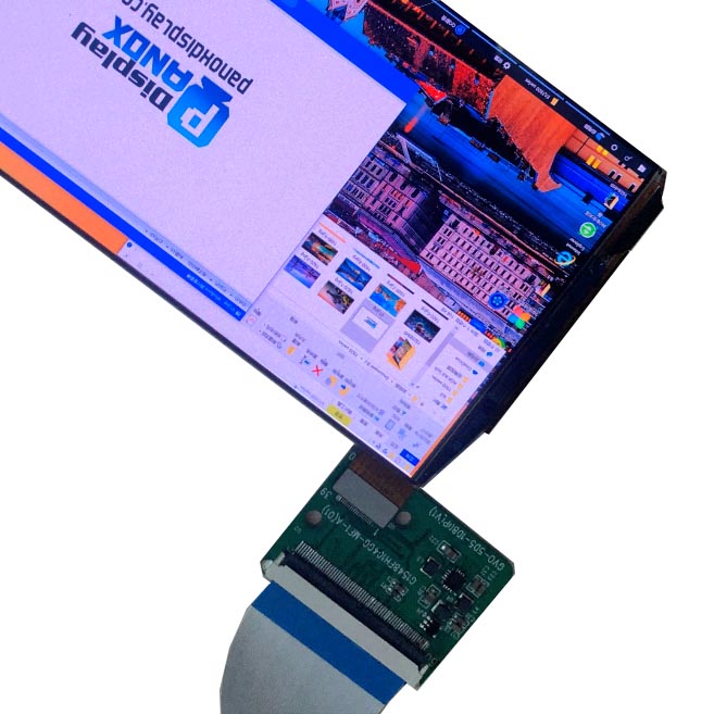
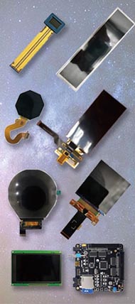
oled display with mipi interface
1. MIPI Source
The MIPI interface was created in 2003 by ARM, Alliance formed by TI, The purpose is to bring up the various interfaces inside the phone (camera CSI, display screen DSI, RF/baseband interface, DigRF, etc.) Standardization, Thus reducing the complexity of mobile phone design and increasing the design flexibility, Currently, the more mature interface applications have DSI (display interface), And the CSI (camera interface), Both have a relatively complex protocol structure, The following figure shows that a certain SOC can act as a receiver for a CSI, Can also act as an exporter for a DSI, Its physical layer uses the D-PHY, Currently the new physical layer C-PHY is also gradually adopted, The Camera I2C interface has a special CCI (Camera Control Interface) in the MIPI to correspond to it2. Display specification standards of the MIPI Alliance
DCS(Display Command Set)To display the standardized command sets in the module command mode;
DBI, DPI (Display Bus Interface, Display Pixel Interface)
DBI: parallel interface with display module with a display controller and frame buffer.
DPI: Parallel interface with the display module, without a display controller or frame buffer.
DSI, CSI (Display Serial Interface, Camera Serial Interface)
DSI: High-speed serial interface between the host processor and the display module;
CSI: High-speed serial interface between the host processor and the camera module;
D-PHY
Provide a physical layer pathway definition for the DSI and CSI;
2.1 DSI / CSI stratification
DSI stratification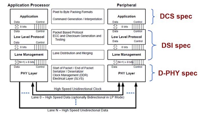
CSI stratification
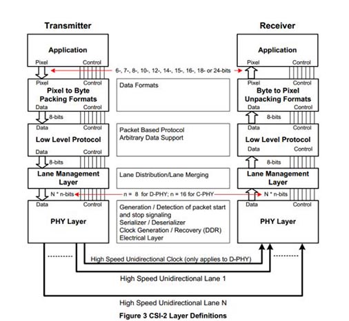
The CSI and DSI stratification are similar
DCS spec: Various algorithm modules for processing the raw image data
DSI / CSI spec: data segmentation and restructuring, and then according to the data type of Baotou, according to the data content of the check sequence, Baotou, data itself, tail, reasonable allocation of data to each channel, after the data through digital to analog conversion into the physical layer (D-PHY) transmission, receiver after receiving the physical layer data, according to the previous reverse package the original data
D-PHY spec: generates the final MIPI waveform
3. MIPI D-PHY
3.1 D-PHY configuration
D-PHY needs one clock channel and one or more data channels, and all data channels need to support high-speed data transmission and forward Escape mode. Data channels are divided into two types of data channels: bi-directional, where bidirectional is semi-bidirectionalNote: The two-way data channel shall include the following functions: (1) reverse transmission of data in HS mode; (2) reverse Escape mode in LP mode;
Configuration Options:
1. One or more data channels;
2. Two-way or one-way data channels on each channel;
3. Inverse communication type supported by each channel;
4. Function of Escape mode in each direction of each channel;
5. Data encoding mode; raw or 8b9b encoding;
1. One or more data channels;
2. Two-way or one-way data channels on each channel;
3. Inverse communication type supported by each channel;
4. Function of Escape mode in each direction of each channel;
5. Data encoding mode; raw or 8b9b encoding;
3.2 Working mode of D-PHY
MIPI D-PHY Introduce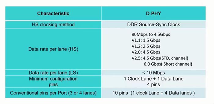
The MIPI D-PHY clock works similar to the DDR clock working mode, Within a single clock cycle, Data were collected along both the ascending and descending edges, Both High speed (HS) and low power (LP) work methods and The maximum data transmission rate supported by HS is 80Mbps-4.5Gbps, The LP mode maximum rate reaches 10Mbps, The two working modes work together, High data transfer is transferred from LP mode to HS mode, When the data is transferred from HS mode to LP mode, Reduce the power consumption, Generally use 1 pair of clock lane with 4 pairs of data lane, The 10 pin feet are needed here
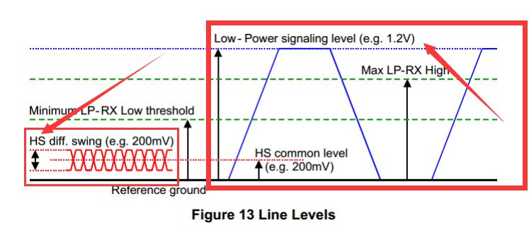
HS high-speed transmission mode: for transmitting burst data, synchronous transmission, the signal is a differential signal, level range of 100mV-300mV, transmission speed range is 80M-1Gbps, when transmission in this mode when the difference line receives 300mV signal, the negative terminal receives 100mV signal, the receiving terminal is recognized as 1, otherwise 0
LP low power mode: for transmission control instructions, asynchronous transmission, the signal is a single terminal signal, level range of 0-1.2V, no useful clock line, the clock is through two data lines different speed less than or equal to 10Mbps, when transmission in this mode, when the positive terminal received 1.2V, receiving terminal recognition 1 when negative terminal received 0V, otherwise 0
What is D-PHY?
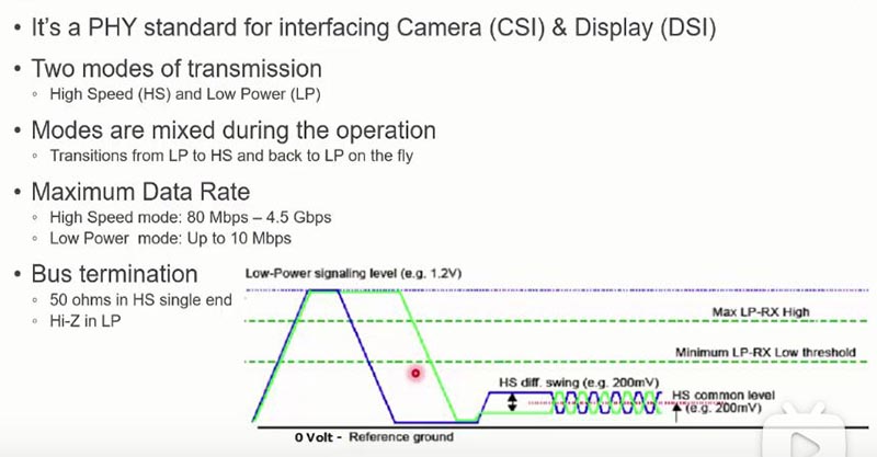
In HS mode, data and clock lane single terminal 50ohms resistance, in LP mode, when no data, D +, D-work in the high-level state of LP, a single end signal, when high data transmission is required, will pass a certain timing of HS mode, HS mode D +, D-is a pair of differential signals
D-PHY Lane Module Functions
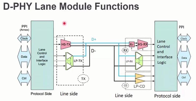
Specific to each implementation on the lane, the left is the master terminal, requiring HS-TX, LP-TX, the two modules connected to the same data line corresponding to the HS-RX and LP-RX to the slave terminal, the slave terminal needs a terminal resistance, and the LP-CD used to check the status of the LP.
4. Schematic diagram of the two D-PHY modes
4.1HS pattern
Below the left for the sending data end, namely master, there are two similar push-pull structure, on the right for the differential signal receiver, composed of two-terminal resistance and terminal enabling signal, working mode is: differential D + signal as an example, when K2 and K4 are open, the voltage connected to the terminal resistance, when the terminal enabled, upper and down two terminal resistance formed circuit, which formed a positive differential signal, when K2, K4 closed, the difference signal negative change, D-controlled by K1 and K3, is an opposite process.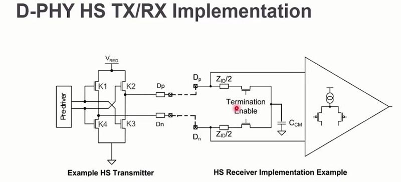
4.2LP pattern
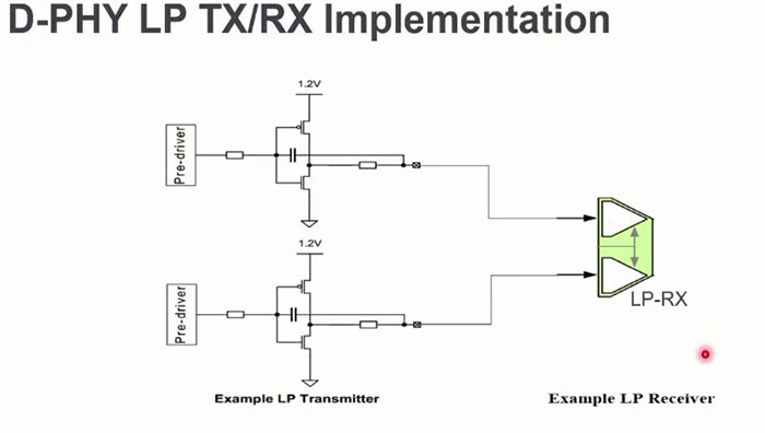
Different from HS mode, RX end does not need terminal, is infinite, only need to control the TX end to make the corresponding change, when the output LP high, namely. output 1.2V, only need to control the above switch open, D + is 1.2V, when need to control output low level, the following switch, so as to realize the low endpoint voltage, so as to achieve voltage change, D + and D-for single end signal in LP mode, so D + and D-can be controlled separately.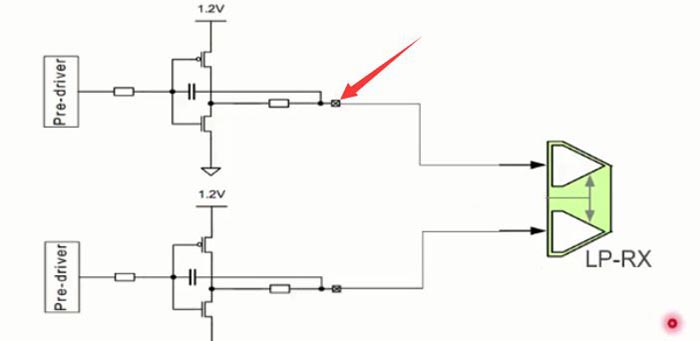
5. Schematic of data transfer of three working modes of D-PHY
5.1 Clock continuous mode
Clock continuous mode is also called HS-TX or burst (burst) mode. As can be seen from the figure, the clock is always present and in differential state. When there is no data transmission, data lane is in lp11 mode, D +, D-are at high level. When data transmission, enter HS mode from LP01 to the LP00 state, and then pass THS-ZERO state, and also exit in a certain sequenceD-PHY LP TX/RX Implementation
Enter the exit command: enter: LP-11, LP-01, LP-00, SoT (00011101); exit: EoT, LP11
5.2 Clock Common mode (non-continuous clock mode)
In normal mode of the clock, the clock lane is in high configuration, making the clock lane in low power mode, clock lane enters HS mode before data lane when data is transmitted, clock lane enters LP mode after data lane, so clock lane is not continuous at this time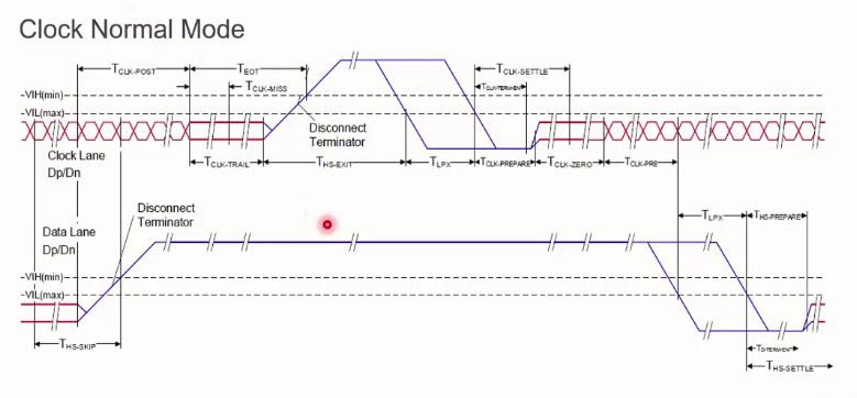
5.3 Escape mode
Data can also be transmitted in LP mode. This working state is called Escape mode. The entry sequence is to enter the escape mode according to the time sequence of the following red frame in LP mode, and then transmit the corresponding data. His clock is obtained through D + and D-, and is mainly used for the transmission of low-speed signals, such as the initialization of the chip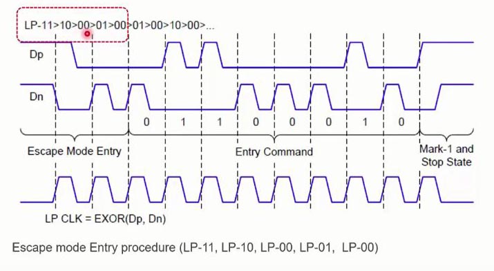
Enter: LP-11, LP-10, LP-00, LP-01, LP-00; exit: LP10, LP11
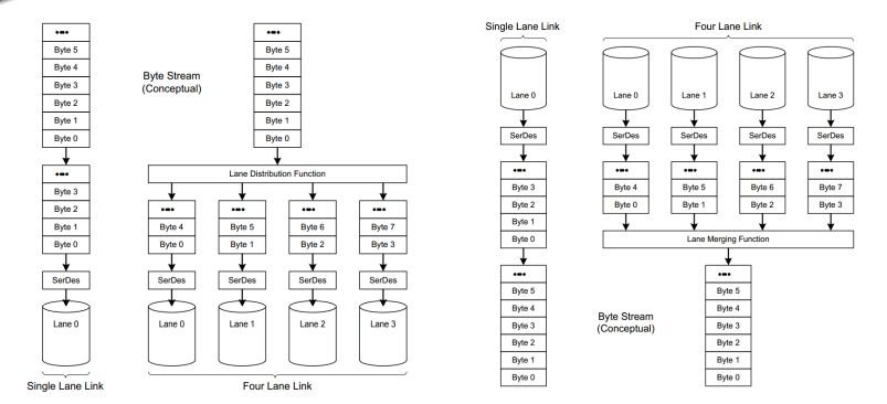
6. MIPI multi-channel allocation and consolidation
For D-PHY, clock data can support up to 4 pairs of data lanes, and the following is the data transmission on D-PHY with different lanes. The sender transfers the data to the receiver through serial rotation, and the receiver parses the data through reverse order