



A TFT LCD module may operate from a 3.3V or 1.8V power supply, yet the thin-film transistors inside the panel often require much higher positive and negative voltages to switch correctly. The gate-on voltage (VGH) may reach +15V to +25V, while the gate-off voltage (VGL) can fall to -5V or -15V, depending on the panel design.
This raises a practical question: if the mainboard only supplies a few low-voltage power rails, where do the higher VGH and VGL voltages come from?
The answer lies in the LCD power management circuitry. Many TFT LCD modules generate these voltages locally through charge pumps and other voltage conversion circuits integrated into the display driver IC or a dedicated power management IC (PMIC).
Understanding this process is useful when troubleshooting white screens, abnormal image colors, excessive voltage ripple, poor black levels, and other display problems that may originate from unstable gate-driving voltages.
What Power Supply Voltages Does a TFT LCD Module Typically Use?
Modern TFT LCD modules commonly use low-voltage inputs supplied by the host system or controller board. The exact configuration varies with the display driver architecture, resolution, panel size, and power requirements.
For many compact displays, a supply between 2.8V and 3.3V is sufficient to operate the driver IC and its associated circuitry. Some modules use two separate supplies, such as 3.2–3.3V for analog or driver functions and 1.8V for the digital interface.
Other modules, particularly certain medium-sized and higher-resolution displays, use a three-power-rail configuration consisting of approximately 1.8V, +5V to +5.5V, and -5V to -5.5V. In these designs, the positive and negative supplies, commonly identified as VSP and VSN, provide power for the analog driving circuitry.
The backlight is usually powered through a separate LED driving circuit, although some modules integrate backlight control into the same electronics.
These configurations are common examples rather than fixed rules. A display larger than five inches does not necessarily require three external supply rails, and a smaller panel is not always limited to a single 3.3V input.
The distinction is important because the voltages supplied through the module connector do not necessarily represent every voltage used inside the panel.
For a broader explanation of LCD power inputs, see What Are LCD Voltage Inputs and How Do They Affect LCD Display Performance?.
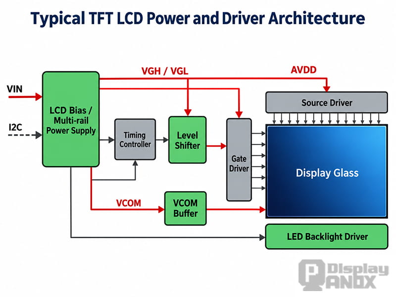 Typical TFT LCD power architecture illustrating the LCD bias supply, gate and source drivers, VGH, VGL, AVDD, and VCOM.
Why Do TFT LCDs Need VGH and VGL Voltages?
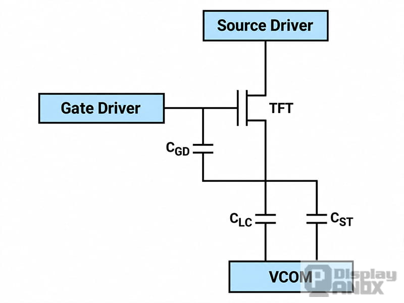
TFT LCD subpixel equivalent circuit showing the gate driver, source driver, liquid crystal capacitor, storage capacitor, and VCOM reference.
A TFT LCD contains an active matrix of thin-film transistors, with each transistor controlling the charging of an individual pixel or subpixel.
The gate driver selects rows of transistors, while the source driver supplies the image data voltages. When a row is selected, its transistors turn on and allow the pixel electrodes to charge to their required levels. When the row is deselected, the transistors turn off so that the stored pixel voltages can be maintained until the next refresh cycle.
This switching process requires two gate-driving voltage levels.
VGH: The Gate-On Voltage
VGH stands for Gate High Voltage, also called the gate-on voltage or VGON.
It provides the positive voltage required to turn on the TFT transistors during row scanning. Depending on the panel, VGH may be approximately +15V, +20V, or even higher.
The gate voltage must be sufficiently high relative to the transistor's source potential to allow proper conduction. If VGH is too low or cannot maintain its specified level under load, the selected transistors may fail to charge the pixel electrodes completely within the available row-selection time.
The resulting display abnormalities can include incorrect pixel voltages, reduced image quality, missing image information, or unstable display patterns.
VGL: The Gate-Off Voltage
VGL stands for Gate Low Voltage, also called the gate-off voltage or VGOFF.
Unlike VGH, VGL is generally negative in conventional TFT LCD gate-driving systems. Depending on the panel design, it may range from approximately -5V to -15V or lower.
Its purpose is to keep unselected TFT transistors reliably turned off, reducing unwanted current leakage from the pixel storage nodes.
If VGL is not sufficiently negative, some transistors may not remain completely off. Excessive leakage can disturb the stored pixel voltages and contribute to image retention, poor contrast, unstable grayscale performance, or abnormal dark-state appearance.
The required VGL level depends on the TFT characteristics and the panel's driving conditions. Applying a more negative voltage than specified does not necessarily improve performance and may exceed the device's operating limits.
VCOM: The Common Electrode Voltage
In addition to VGH and VGL, TFT LCD panels require a common electrode voltage known as VCOM.
VCOM provides a reference potential for the liquid crystal cells. The effective voltage across each liquid crystal cell depends on the difference between the pixel electrode voltage and the common electrode voltage.
An incorrectly adjusted or unstable VCOM voltage may cause visible flicker, image sticking, or uneven grayscale behavior.
VCOM is commonly generated using a programmable reference, resistor-divider network, or digital-to-analog converter, together with a buffer amplifier capable of driving the common electrode load.
Unlike VGH and VGL, which primarily control TFT switching, VCOM directly affects the voltage applied across the liquid crystal layer.
How Are VGH and VGL Generated from a Low-Voltage Supply?
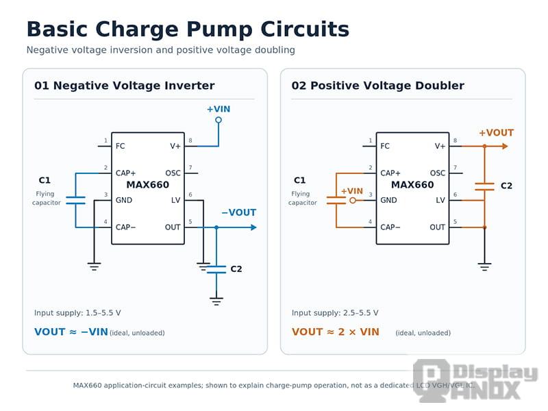
Basic charge pump circuits demonstrating positive voltage doubling and negative voltage inversion using switched capacitors.
The most common approach to generating the positive and negative gate voltages is a charge pump circuit.
A charge pump is a switched-capacitor voltage converter. It transfers electrical charge between capacitors through a controlled network of switches, allowing the circuit to produce voltages higher than the input supply or voltages with the opposite polarity.
Unlike a conventional inductor-based boost converter, a basic charge pump uses capacitors as its main energy-transfer components.
How a Positive Charge Pump Generates VGH
The operation of a positive charge pump can be understood through a simple voltage-doubling circuit.
During the first switching phase, a capacitor is connected across the input supply and charged to approximately the input voltage.
During the second phase, the switching network changes the capacitor's connections so that its stored voltage is placed in series with the input supply. Ideally, this arrangement can produce an output approaching twice the original supply voltage.
For example, a 5V input can theoretically produce nearly 10V through a voltage-doubling stage. By cascading additional stages or using a different charge-pump configuration, higher voltages can be generated.
Actual output voltages are lower than the ideal values because of switching losses, capacitor characteristics, load current, and other circuit limitations.
In a TFT LCD power supply, a positive charge pump may generate the VGH rail from an existing analog supply or from the output of a preceding boost converter.
The converter's regulation circuitry then maintains the required gate-on voltage as the load changes.
How a Negative Charge Pump Generates VGL
A negative charge pump operates on a similar principle but uses a different switching arrangement to reverse the output polarity.
A capacitor is first charged from the available positive supply. The switching network then reconnects the capacitor so that the output node is driven below the ground reference.
With suitable circuit stages and regulation, the converter can generate the negative voltage required for VGL.
For example, a circuit operating from a positive supply may produce a regulated negative gate-off voltage such as -7V or -10V.
Both positive and negative charge pumps can be included within the same display power management IC. Depending on the design, the IC may also integrate switching controls, voltage regulators, protection circuits, and the circuitry used to establish VCOM.
This explains why a display module can operate with only a few low-voltage inputs while still producing the substantially different voltages required by its internal TFT matrix.
However, charge pumps are not the only voltage conversion method used in LCD systems. Inductor-based boost converters and inverting DC-DC converters are also common, especially when higher output currents or additional analog supply rails are required.
Why Are ±15V Supplies Not Usually Connected Directly to the Display?
The absence of +15V and -15V pins on a display connector does not mean these voltage levels are unnecessary.
It often means the module's power architecture generates the required voltages internally.
For example, a display module may receive a 3.3V input from the host board. Inside the module, a power management circuit can boost that voltage to supply the analog driver circuitry, then generate the higher positive and negative gate voltages through additional conversion stages.
In another architecture, the host board provides 1.8V logic power together with positive and negative analog supplies of approximately ±5.5V. The display driver circuitry then produces the gate-driving voltages required by the TFT array.
The externally supplied ±5.5V rails should not be confused with VGH and VGL. They may serve as source-driver analog supplies, while the actual gate voltages are generated separately.
Some larger TFT LCD panels use an external PMIC or dedicated power supply board to generate VGH, VGL, AVDD, and VCOM. Other modules integrate part or all of this circuitry into their driver electronics.
Therefore, whether these voltages are generated inside the display driver IC, on the module PCB, or by an external power circuit depends on the specific panel architecture.
How LCD Power Supply Integration Has Changed
Earlier TFT LCD designs often relied on relatively visible external power conversion circuits.
A typical module PCB could contain a dedicated boost converter, charge-pump capacitors, inductors, diodes, voltage-setting resistors, and other components needed to generate VGH and VGL.
These circuits occupied space and required careful component selection and PCB layout. Engineers could often identify the voltage-generation stages directly by examining the module's circuit board.
Modern display driver ICs integrate an increasing number of these functions. In some compact LCD modules, the voltage-generation circuitry is incorporated into the driver IC, reducing the need for separate power management components.
As a result, certain low-power displays may have very few visible external components associated with their gate-driving supplies.
This integration reduces PCB area, simplifies assembly, and can lower the overall component count.
Nevertheless, integration does not eliminate every external component. Charge pumps may still require external flying capacitors or output capacitors, while higher-power converters may need inductors and additional filtering components.
The degree of integration also depends on the display's current requirements. Larger or more demanding panels often retain dedicated power management circuits because their analog supply rails require greater current capacity and tighter regulation.
Although modern IC integration has simplified the visible hardware, the underlying voltage-generation requirements remain important during LCD module development and troubleshooting.
Common VGH and VGL Problems in TFT LCD Displays
Unstable gate-driving voltages can cause a range of image abnormalities. These problems are sometimes mistaken for software initialization errors, incorrect display timing, or defective LCD panels.
A practical diagnosis should examine the relevant power rails before changing display driver registers.
Insufficient VGH Voltage: White Screens and Abnormal Images
One possible cause of an abnormal display is insufficient VGH voltage.
When the positive gate voltage cannot reach its required level, the TFT transistors may fail to turn on strongly enough during row selection. The source driver then has difficulty charging the pixel electrodes to their intended voltages.
Depending on the display mode and panel architecture, the symptoms may include a white or washed-out screen, missing image areas, flickering, or distorted patterns.
The key measurement is not simply whether VGH exists, but whether it remains within specification while the panel is operating.
A charge-pump circuit may produce the expected voltage with little or no load but fail to maintain that voltage when the gate driver begins switching.
This condition can result from insufficient converter current capability, excessive loading, a defective capacitor, or a problem in the voltage regulation circuit.
Excessive VGH Ripple: Check the Charge-Pump Capacitors
A useful troubleshooting method is to observe VGH with an oscilloscope.
Some switching ripple is normal in charge-pump circuits. However, excessive ripple, repeated voltage collapse, or unusually large sawtooth-shaped fluctuations may indicate that the voltage-generation stage is struggling to maintain regulation.
In designs that use external capacitors, one possible cause is an incorrect or insufficient charge-pump capacitance.
A flying capacitor transfers charge between stages during each switching cycle. If its effective capacitance is too small, the converter may transfer insufficient charge to maintain the output voltage under load.
An output capacitor also helps smooth the generated voltage and supply transient current.
A missing, poorly soldered, damaged, or incorrectly specified capacitor can therefore cause unstable output voltage or excessive ripple.
Ceramic capacitor selection deserves particular attention because the effective capacitance of some multilayer ceramic capacitors decreases significantly under DC bias.
During hardware debugging, measuring the actual capacitance of accessible external components can sometimes reveal a problem more quickly than repeatedly changing driver IC registers.
In an appropriate engineering test setup, temporarily substituting a correctly rated capacitor may help confirm whether a component-value problem is responsible.
However, additional capacitance should not be added arbitrarily. Some LCD power IC outputs, particularly gate-voltage shaping outputs, have specific restrictions on external capacitance. The circuit must follow the IC manufacturer's recommended configuration.
Insufficiently Negative VGL: Pixel Leakage and Poor Black Levels
VGL problems can be less obvious than complete power failure.
If the negative gate-off voltage is too close to zero, the TFT transistors may not remain fully turned off during the holding period.
This can allow unwanted leakage current to alter the charge stored at the pixel electrodes.
Depending on the panel design, the resulting abnormalities may include unstable grayscale levels, image retention, contrast degradation, or dark areas that appear lighter than expected.
A display that cannot maintain a stable black image should therefore be checked for VGL abnormalities, although backlight leakage, liquid crystal characteristics, VCOM adjustment, gamma settings, and other factors can produce similar symptoms.
A VGL measurement should include both the DC voltage level and its stability during normal operation.
If VGL becomes less negative under load or shows abnormal ripple, the negative voltage-generation circuit and its supporting components should be investigated.
A Practical Troubleshooting Approach for LCD Gate Voltages
When a TFT LCD displays a white screen, distorted image, excessive flicker, or poor contrast, the power supply is a reasonable starting point for diagnosis.
The first step is to verify that the module receives the correct external supply voltages. Depending on the design, these may include VCI, IOVCC, VSP, VSN, or other specified power inputs. The backlight supply should be checked separately because a functioning backlight does not confirm that the TFT driving circuitry is operating correctly.
Once the input supplies are confirmed, VGH and VGL can be measured at the designated test points, where accessible. Their values should be compared with the panel datasheet rather than with assumed universal voltage levels.
An oscilloscope is particularly useful because it can reveal ripple, voltage collapse, or startup instability that a digital multimeter may not show.
If VGH is unstable, the positive charge-pump or boost stage should be examined. If VGL is abnormal, attention should turn to the negative voltage-generation circuit. Where external components are used, capacitor values, solder joints, diodes, inductors, and feedback components should be checked according to the circuit design.
VCOM should also be measured when the display exhibits flicker, image retention, or grayscale problems.
Another important factor is power sequencing. TFT LCD power management ICs frequently control the order in which analog, gate-driving, and reference voltages are enabled or disabled. Incorrect sequencing can produce startup problems even when the final steady-state voltages appear normal.
These measurements should be performed using suitable probes and the manufacturer's recommended test points. High-voltage bias circuits and sensitive driver outputs can be affected by inappropriate probing or added capacitance.
If all supply rails are correct and stable, the investigation can proceed to the display interface, initialization commands, timing signals, and panel connections.
The relationship between the controller board and display module is covered in Why Does an LCD Need a Controller Board or Driver Board?.
Why VGH and VGL Still Matter in Modern LCD Design
With modern driver ICs, much of the LCD power conversion circuitry is hidden inside highly integrated semiconductor devices. A compact display may expose only a few supply pins, even though its internal TFT driving system operates across a much wider voltage range.
This makes module integration easier, but it can also make power-related faults less visible.
A display may receive the correct 3.3V or 1.8V input, its backlight may illuminate normally, and the communication interface may operate correctly, while the gate-driving voltages remain unstable.
Understanding how VGH and VGL are generated helps distinguish these electrical faults from problems caused by display software or image data.
For engineers selecting or integrating TFT LCD display modules, checking the required input supplies, internal bias architecture, gate-driving voltages, and startup sequence is an important part of ensuring reliable operation.
Conclusion
The high positive and negative voltages required by TFT LCD gate drivers do not always need to be supplied directly by the host system.
In many modern LCD modules, VGH and VGL are generated from lower-voltage power rails through charge pumps, boost converters, or other integrated power management circuits. VCOM is established through a separate reference and buffering arrangement to support stable liquid crystal driving.
Earlier designs commonly used more discrete external components, while newer driver ICs integrate much of the voltage-generation circuitry.
When a display develops a white screen, unstable image, excessive ripple, or poor dark-state performance, checking VGH, VGL, VCOM, and their associated power circuits can help identify the underlying fault.
A systematic examination of these voltages often provides a clearer diagnosis than adjusting display driver registers without first confirming that the hardware is operating correctly.