



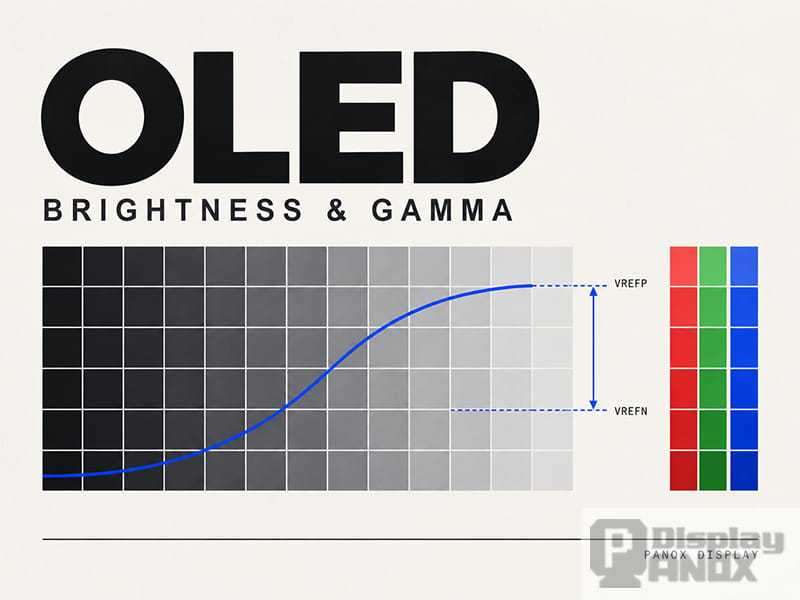
Two OLED displays can have the same resolution and rated brightness yet produce noticeably different images. One may show smooth shadow transitions, while another loses dark detail or develops a color tint at low brightness. These differences can arise from the reference voltages, gamma settings, and calibration data used to drive the panel.
VREF, VREFP, and VREFN are terms that appear in OLED driver documentation. Understanding their functions helps explain how digital grayscale values become electrical driving signals—and why those signals must be matched to the characteristics of the panel.
What Does VREF Mean in an OLED Display?
VREF generally stands for reference voltage. A reference provides a stable electrical basis for other circuits inside the display driver IC, or DDIC. Depending on the chip architecture, it may support voltage generation, analog conversion, regulation, or panel-driving functions.
In an AMOLED display, the source driver converts digital image data into analog voltages. The pixel circuit uses these voltages to control the current through the OLED emitter. Gamma settings shape the relationship between the incoming grayscale code and the resulting luminance.
An inaccurate or unstable reference can therefore affect many grayscale levels at once. The image may become too bright, lose tonal separation, or change color as operating conditions vary. PANOX Display’s explanation of OLED display driver IC architecture describes how reference generation, source driving, and pixel compensation work together.
However, VREF is not a universal name for the entire grayscale voltage range. A signal called VREF may be a single internal reference voltage, while the gamma circuit uses separately named upper and lower references. The exact function comes from the DDIC specification.
VREFP and VREFN: Understanding the Reference Window
A useful way to understand reference-voltage adjustment is to consider two electrical boundaries and the voltage window between them.
Where VREFP and VREFN are defined as the upper and lower boundaries of that window, its width is:
ΔVREF = VREFP − VREFN
Here, ΔVREF means the difference between the two reference levels. It should be distinguished from a physical pin or register simply named VREF.
The window has two properties: its width and its position. Its width describes the separation between the boundaries. Its position describes where that range sits relative to ground or another circuit reference. Both can influence the operating conditions of the driver and pixel circuit.
The names require care. Some AMOLED drivers use VREFP/VREFN-family signals for panel reference or initialization functions, while gamma endpoints have names such as VGMP and VGSP. Other OLED architectures use several gamma reference points rather than a single pair.
The Sony ECX331DB, for example, identifies separate gamma references associated with grayscale codes 255, 128, 32, and 1, together with an offset associated with code 0. Its manufacturer datasheet hosted by PANOX Display shows why reference functions must be interpreted within the specific panel architecture.
The same distinction applies to brightness direction. A higher electrical voltage does not always produce a brighter OLED pixel. The response depends on transistor polarity and pixel-circuit design. VREFP should therefore not automatically be treated as the white-level control, or VREFN as the black-level control.
How Reference Voltages Affect OLED Gamma Correction
An 8-bit color channel contains 256 digital codes, from 0 to 255. Those codes do not necessarily correspond to 256 evenly spaced driving voltages.
The driver maps each code to an electrical output according to its gamma settings. This mapping accounts for the nonlinear relationship between data voltage, transistor current, and OLED luminance.
A simplified reference-window model can be written as:
VOUT(g) = VLOW + F(g) × (VHIGH − VLOW)
In this model, g is the grayscale code, and F(g) represents the programmed mapping within the voltage range. It need not be linear, and its direction depends on the driving architecture.
This explains why reference voltages and gamma settings must be considered together. The reference range establishes electrical boundaries; the gamma mapping determines how grayscale levels are distributed within them.
For example, the BOE BO139A454SPI specification documents separate red, green, and blue gamma correction and evaluates the gamma curve at multiple grayscale codes. Matching maximum white brightness alone does not establish that the intermediate levels or color balance are correct.
Two Ways to Adjust a Reference Window
Reference-window adjustment can be understood through two operations: shifting the range and changing its width. These describe electrical behavior. Their effect on the visible image must still be measured.
Shifting Both Reference Levels
If both endpoints move by the same amount, their difference remains unchanged:
(VREFP + ΔV) − (VREFN + ΔV) = VREFP − VREFN
For example, moving an illustrative window from 1.0–5.0 V to 1.2–5.2 V preserves its 4.0 V width.
In a simplified model with an unchanged gamma mapping, this shifts the output-voltage range without changing its relative spacing. It can be useful when adjusting the electrical operating point.
Preserving that spacing does not guarantee an unchanged optical gamma curve. The pixel transistor responds to voltage differences within its circuit, and its current response is nonlinear. An electrical offset may therefore affect shadows, midtones, and highlights differently.
The appropriate check is the measured luminance curve, rather than the reference difference alone.
Expanding or Compressing the Range
Changing one endpoint, or moving the endpoints by different amounts, changes the window width.
In the same illustrative example, changing 1.0–5.0 V to 1.0–5.2 V expands the range from 4.0 V to 4.2 V. Moving the upper endpoint to 4.8 V compresses it to 3.8 V.
With the mapping otherwise unchanged, these adjustments alter the electrical separation between grayscale outputs. They can affect drive range, tonal response, and the margin available near an endpoint.
A wider range does not automatically produce smoother gradients, and a narrower range does not always produce a washed-out image. Grayscale quality also depends on DAC accuracy, gamma control points, reference noise, and the panel’s current response. Changing the range may require further gamma adjustment to preserve the intended luminance progression.
Why OLED Panels Need Individual Calibration
OLED manufacturing introduces variation even among panels made to the same design.
The driving TFTs can differ in threshold voltage and carrier mobility. Variations in organic-layer deposition can affect emitter characteristics. Storage capacitance, parasitic coupling, and resistance in the panel wiring can also influence how accurately a pixel is programmed and driven.
As a result, the same nominal data voltage may not produce exactly the same luminance on every panel. These differences can become particularly visible near black, where the intended emission current is very small.
Factory calibration measures the panel’s optical response and adjusts the available controls to bring brightness, gamma, and color coordinates within the specified tolerances. Depending on the design, those controls may include reference-voltage trims, RGB gamma tables, channel gains, offsets, or spatial compensation data.
The resulting settings can be stored in OTP, MTP, EEPROM, or another nonvolatile memory. The Sony ECX331DB documentation, for instance, describes EEPROM settings used to adjust luminance and white chromaticity.
Individual calibration does not necessarily mean that every panel receives a unique pair of VREFP and VREFN values. The parameters used depend on the driver and production process.
Global reference adjustment also has limits. It can help align the overall response between panels, but local bright or dark regions may require pixel or region compensation. A single reference pair cannot independently correct every area of a display.
Reference-Voltage Errors and Common OLED Image Problems
Unsuitable reference or gamma settings can appear as poor shadow detail, washed-out midtones, highlight compression, or color differences between panels. These symptoms provide useful starting points for diagnosis, but they do not identify a particular reference signal on their own.
| Visible problem | Reference and calibration checks |
|---|---|
| Washed-out image or weak tonal separation | Check the effective drive range, gamma mapping, and black-level offset. |
| Excessive brightness or lost highlight detail | Check high-gray mapping, endpoint limits, and RGB channel balance. |
| Banding, crushed shadows, or raised blacks | Check low-gray control points, reference stability, and near-black pixel behavior. |
| Color differences between otherwise similar panels | Check RGB gamma settings, white-point calibration, and the correct panel-specific data. |
Near-black errors deserve particular attention. Several neighboring codes may produce almost indistinguishable luminance, making a gradient appear stepped or causing dark details to disappear. Differences between the RGB channels can also introduce a tint into neutral gray.
A useful evaluation combines stepped grayscale patterns, smooth ramps, and individual RGB patterns. Testing at more than one brightness setting helps reveal behavior that a full-white image can hide.
Temperature and operating mode also matter. A calibration that performs well under one condition may not track identically under another. The Sony module documentation explicitly includes temperature compensation through its gamma-top reference.
Reference settings should be examined alongside power stability, initialization data, and display timing. Changing voltage parameters before confirming those conditions can obscure the actual cause of an image problem.
Applying These Principles to OLED Module Integration
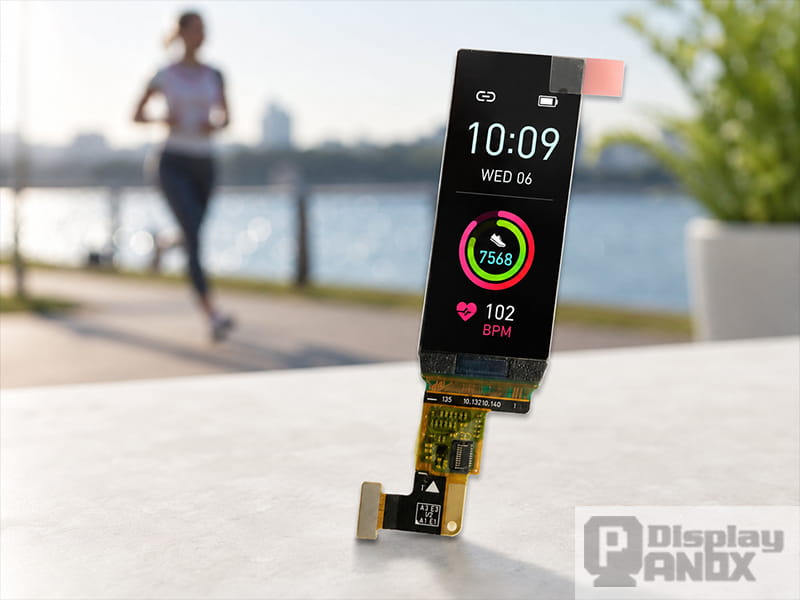
1.91 inch OLED For Wearable Smartwatch
For PANOX Display integration projects, the panel and its driver specifications need to be reviewed together. Size, resolution, and connector appearance provide only part of the information required to reproduce the intended image quality.
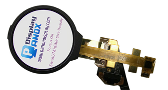
The 1.39-inch round AMOLED product page, for example, lists AUO and EDO options with the same 400 × 400 resolution but different driver ICs and connector definitions. Similar display dimensions do not make their initialization or calibration settings interchangeable.
For compact rectangular designs, the 1.91-inch 240 × 536 AMOLED module offers another MIPI display format. Its electrical requirements and supplied configuration should be evaluated as part of that specific module.
VREF, VREFP, and VREFN are useful starting points for understanding OLED image quality, provided their roles are established from the correct documentation. Reference-window position and width influence the electrical operating range; gamma mapping and panel calibration determine how that range becomes visible brightness and color. Reliable results come from matching those settings to the panel and verifying the full grayscale response.