


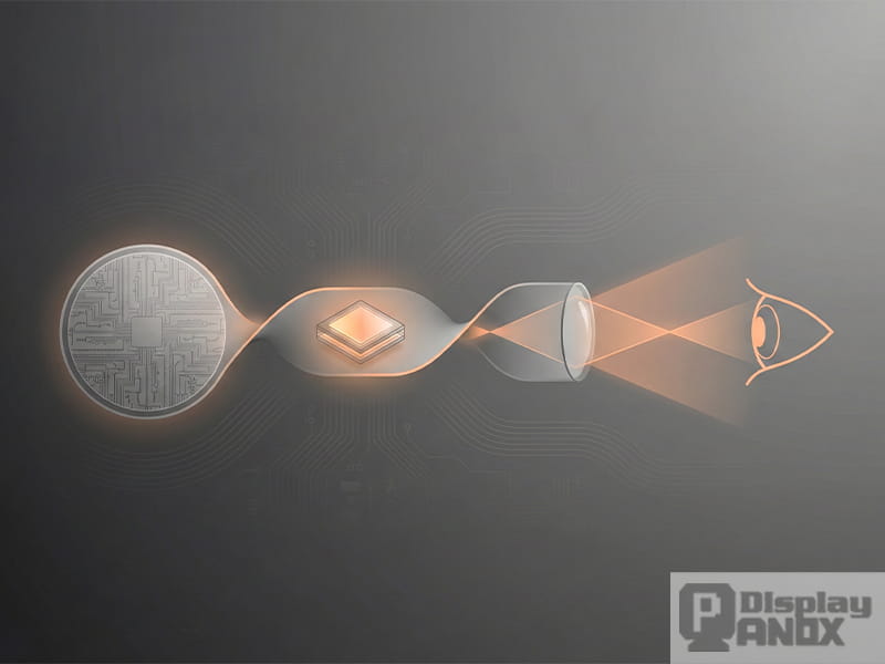
Micro OLED (often called silicon-based OLED or OLED-on-silicon) is widely used as a core visual component in VR/AR near-eye systems because it can deliver ultra-high brightness, extremely fine image quality, and a very small form factor—all enabled by tightly controlled semiconductor and thin-film processes.
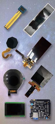
Explore More Displays for AR/VR Applications
Device Architecture: The Four-Layer Stack
A silicon-based Micro OLED can be understood as a precision “layer cake” built on top of a silicon wafer:
-
Silicon substrate / backplane (with integrated circuits): provides mechanical support and pixel-driving circuitry.
-
Anode layer (often ITO or related transparent conductive stack): injects holes.
-
Organic emissive layers: emit red/green/blue light (commonly via patterned deposition).
-
Cathode layer (e.g., semi-transparent metal stack such as Mg/Ag): injects electrons while maintaining sufficient optical transmission.
Each functional layer is typically nanometer-scale, and uniformity depends heavily on high-vacuum deposition control.
Backplane Fabrication: CMOS-Grade Silicon Foundation
The backplane is the “brain” that drives each pixel precisely. A standard Micro OLED backplane is CMOS-based on silicon, manufactured using processes that look similar to advanced semiconductor IC fabrication.
Wafer Cleaning
To suppress defects at microdisplay pixel densities, wafers go through rigorous cleaning (e.g., wet clean + ultrasonic assist) and drying/bake steps to remove nanometer-level particles and residues.
Photolithography and Pattern Transfer
Using UV exposure through masks (or equivalent patterning), the process defines dense transistor and interconnect patterns—often millions of devices. This step is repeated many times across layers to build the CMOS pixel-driving circuits.
Ion Implantation and Doping (Electrical Control)
Ion implantation forms doped regions that determine transistor behavior and enables tight current control per pixel. This is one reason Micro OLED can achieve much finer grayscale/current regulation than conventional large-area LCD driving schemes, which helps stabilize brightness and uniformity across a tiny display.
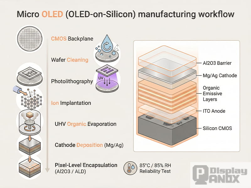
Frontplane Deposition: Vacuum Thin-Film “Art”
After the backplane is prepared, the OLED functional stack is formed on top under carefully controlled vacuum conditions.
ITO Anode Activation (Plasma Treatment)
A plasma or ion-based surface activation step improves hole injection efficiency at the anode interface. This is described as boosting injection efficiency and significantly increasing effective brightness.
Organic Layer Evaporation (Ultra-High Vacuum)
Organic materials are typically deposited by thermal evaporation in an ultra-high vacuum environment. Tooling such as Tokki-type evaporators is commonly used in OLED manufacturing. Deposition control can reach around 0.1 nm/s, and thickness error may be constrained to extremely small margins (within ~3 atomic layers), which is crucial for color stability, efficiency, and lifetime.
Cathode Formation (Semi-Transparent Metal)
A Mg/Ag alloy cathode stack is often created via magnetron sputtering or related deposition methods to achieve a layer that is both conductive and sufficiently optically transmissive, supporting top emission structures widely used in microdisplays.
Pixel-Level Encapsulation: Protecting OLED at the Micron Scale
Moisture and oxygen are the natural enemies of OLED. Micro OLED therefore relies on extremely strict encapsulation.
Atomic-Scale Passivation (Al₂O₃ / ALD-Style Protection)
A dense inorganic barrier such as Al₂O₃ can be deposited to protect delicate OLED structures.This with lifetime improvements up to 30,000 hours under specified conditions.
Ultra-Dry Glovebox Sealing and Inert Gas Fill
Encapsulation is performed in an ultra-dry environment (your material cites a very low dew point), then a glass cap is bonded using UV-curable adhesive. The cavity is filled with an inert gas (commonly nitrogen; in some processes argon may also be used) to reduce oxidation risk.
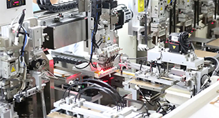
Module Integration: Turning a Wafer into a Usable Microdisplay
Once the OLED stack is complete and sealed, the process transitions from wafer-level fabrication to module-level engineering.
Dicing / Laser Cutting into Microdisplays
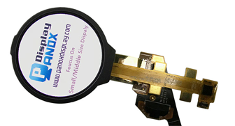
The wafer is diced into individual dies (Highlights 0.39-inch micro screens). Edge quality matters for mechanical yield and optical assembly, so high-precision cutting and polishing approaches are used.
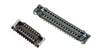
COG Bonding (Chip-on-Glass) and Fine-Pitch Interconnect
To connect the driver IC and/or interposer structures, COG bonding with gold ball bonding is used, with key parameters such as:
-
Gold ball diameter around 60 μm, height around 20 μm
-
First bond push force > 20 gf, overall line pull force > 109 gf
-
Fine interconnect spacing (Highlights 15 μm pitch/spacing)
-
Surface cleanliness control (e.g., plasma/ion cleaning); if the process is delayed beyond 72 hours, low-temperature baking may be used to remove moisture before bonding
These steps directly impact contact reliability, yield, and long-term stability.
Burn-In and Reliability Screening (85°C / 85% RH)
A common accelerated stress test is the 85°C / 85% humidity condition. Uses 500 hours of continuous lighting and notes a reject rate controlled below 0.05% (i.e., less than five in ten thousand).
“Black Tech” Breakthroughs Behind Micro OLED Performance
Vertical Interconnect / Hybrid-Style Bonding Concepts
Describes a “non-aligned bonding” concept enabling precise interconnection between CMOS circuitry and OLED pixels. In practice, advanced microdisplay flows may use wafer-level alignment, fine-pitch interconnects, or hybrid bonding-like approaches to achieve extremely tight registration and low parasitics.
ALD Defect Repair for Yield Improvement
By using ALD (Atomic Layer Deposition) to fill nano-scale pinholes/defects, the process can reduce leakage paths and improve encapsulation integrity. Attributes this to yield reaching ~98%.
Microcavity Spectral Tuning for Wide Color Gamut
Microcavity effects can be used to tune emission spectra and improve color purity/efficiency.The material states color gamut coverage reaching 110% NTSC.
Learn more:Why AR MR Glass Need High Brightness Micro OLED?
Why “200+ Steps” Matters for VR/AR
From wafer prep and CMOS backplane fabrication to vacuum evaporation, pixel-level encapsulation, bonding, and harsh reliability screening, Micro OLED manufacturing can involve 200+ tightly controlled process steps. That complexity is exactly what enables:
-
High pixel density and sharp near-eye imagery
-
Stable brightness and uniformity
-
Strong environmental resistance for long-term operation
- Compact modules that fit tight optical engines in VR/AR devices
If you are seeking high-performance Micro OLED display solutions, we offer a comprehensive range of products for your selection.