


Blue OLEDs have historically been the weak link in OLED screen technology due to their limited lifespan and efficiency. A research team at the University of Michigan has now unveiled a game-changing solution in Nature Photonics: a blue phosphorescent OLED display with a lifetime comparable to commercial green PHOLEDs—a 250x improvement over previous models.
While red and green pixels in an OLED panel typically use highly efficient phosphorescent emitters, blue subpixels have relied on less stable fluorescent materials. This inefficiency has limited the widespread adoption of all-phosphorescent OLED display panels, hindering the development of more power-efficient and durable screens.
Led by Professor Stephen Forrest, the Michigan team addressed the issue by introducing the concept of an “exciton fast lane.” The design couples excitons with surface plasmon polaritons at the metal electrode, forming hybrid particles that accelerate light emission via the Purcell effect. This significantly reduces exciton annihilation—a common degradation issue in small OLED displays used in mobile and wearable devices.
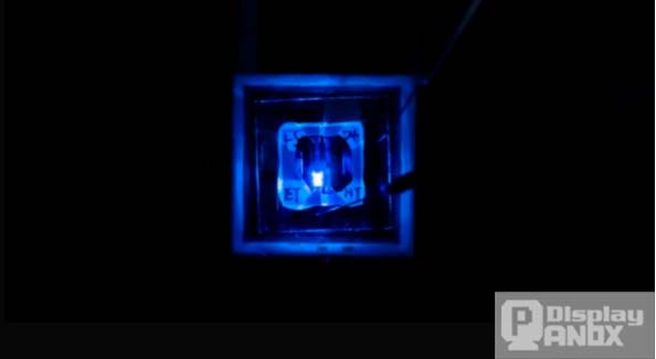
The team implemented this by applying an ultra-thin carbon-based semiconductor layer to the cathode of the custom OLED display prototype. This layer enhances the interaction between excitons and plasmonic fields, allowing energy to be concentrated near the surface where emission is most efficient.
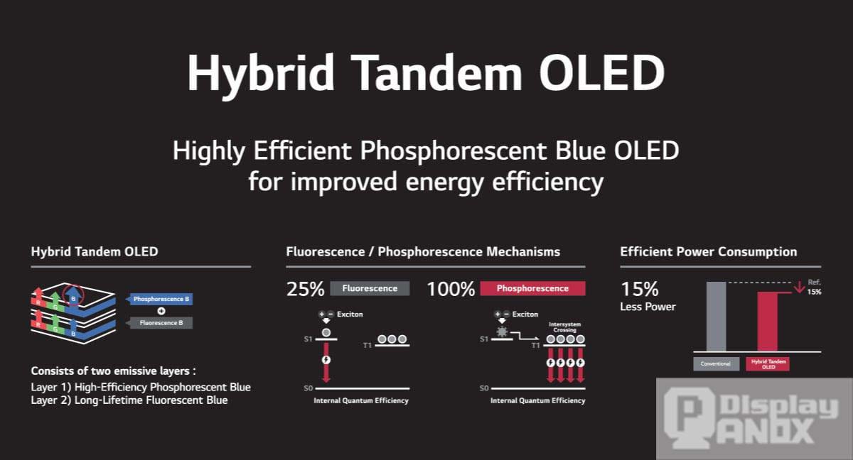
Additionally, a tandem architecture was used with two stacked emission layers. This approach halves exciton density in each layer, further lowering the chance of annihilation and ensuring a more stable OLED screen output. The resulting device acts as both an efficient emitter and an optical cavity, optimizing deep-blue light emission.
The newly developed blue PHOLED matches the brightness and operational stability of commercial green PHOLEDs, a leap toward manufacturing high-efficiency, long-lifespan full RGB OLED panels. These advances will have a direct impact on a wide range of devices—especially small OLED displays used in smartphones, tablets, and custom OLED screens for automotive and test AR/VR applications.
Supported by the U.S. Department of Energy and Universal Display Corporation (UDC), the work was carried out at Michigan’s Lurie Nanofabrication Facility. The patented design has already been licensed to UDC, signaling rapid commercialization potential.
Professor Forrest noted that the work represents a convergence of quantum optics, electrical engineering, and advanced materials science. As development progresses, this technology could define the future of OLED display panels, enabling thinner, more efficient, and color-accurate devices across industries.
With this innovation, the path toward fully phosphorescent OLED displays—delivering higher brightness, better color accuracy, and longer lifespans—is finally within reach, unlocking a new era in OLED screen design.

Specialist LCD/OLED Supplier
|
|

Verification Code*

Panox Display

Browse Articles by Category
OEM SERVICE
Customized Touch Panel
HDMI/Type-C Controller/Driver Board
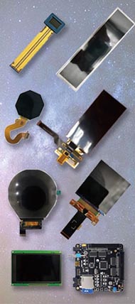
Custmized LCD/OLED
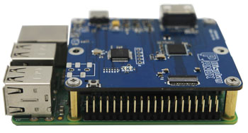
Free Connectors
Find a Display to Fit Your Application
For More OLED/LCD Panels
Get the Latest Displays
If our display fit your application, subscrlbe for monthly Insights
Panox Display Professional OLED/LCD Supplier and Manufacturer
- 📍 Shenzhen
- 📞 Phone: 86 755 3396 6409
- 📠 Skype: panoxwesley
COPYRIGHT © 2015-2025 Panox Electronics Co.,Ltd. ONE-STOP DISPLAY SYSTEM SOLUTION

We got your inquiry and will contact you within one work day.
If it`s urgent, try to contact
Whatsapp: +86 18665870665
Skype: panoxwesley
QQ: 407417798
If it`s urgent, try to contact
Whatsapp: +86 18665870665
Skype: panoxwesley
QQ: 407417798