



Rockchip display bring-up is not the work of a single “screen driver.” A working display depends on an end-to-end path that includes image generation, memory buffers, VOP or VOP2 scanout, a display interface controller, the PHY, power sequencing, and the panel or monitor itself.
Linux organizes this path through the Direct Rendering Manager and Kernel Mode Setting frameworks, usually shortened to DRM/KMS. DRM/KMS represents the hardware as a set of connected objects and uses atomic state updates to keep mode changes, planes, buffers, and output routing consistent.
This guide explains that complete architecture. It covers DRM/KMS objects, Rockchip VOP and VOP2 hardware, display timing, bandwidth, GEM and DMA-BUF, Atomic KMS, Device Tree graph routing, panel sequencing, interface-specific bring-up, modetest, source-code navigation, and systematic display debugging.
The discussion applies broadly to Rockchip platforms such as RK3288, RK3399, RK3566, RK3568, RK3576, RK3588, PX30, RV1103, and RV1106. Exact source paths, node names, debugfs entries, clock trees, and supported features vary by SoC, BSP, and kernel version. Every implementation must therefore be checked against the active SDK, SoC technical reference manual, Device Tree bindings, display datasheet, and board schematic.
1. Understanding the Complete Rockchip Display Pipeline
A displayed frame passes through five distinct stages:
- A CPU, GPU, RGA, video decoder, camera pipeline, or other producer creates an RGB or YUV image.
- The image is stored in a DDR buffer, using either a linear layout or a format modifier such as AFBC.
- VOP or VOP2 reads the buffer through AXI and performs scanout, scaling, alpha blending, color-space conversion, HDR processing, or gamma correction.
- An HDMI, DisplayPort, eDP, MIPI DSI, LVDS, or RGB controller converts the pixel stream into the required interface protocol.
- The PHY generates the electrical signal, and the panel or monitor reconstructs the timing and image.
The complete data path can be summarized as:
CPU / GPU / RGA / VPU
        ↓
DDR Buffer: RGB, YUV, linear layout, or AFBC
        ↓
VOP / VOP2: fetch, scale, compose, CSC, HDR, gamma
        ↓
Video Port
        ↓
HDMI / DP / eDP / MIPI DSI / LVDS / RGB controller
        ↓
PHY, cable, connector
        ↓
Panel or monitor
This distinction matters because each block has a different failure mode. A correct framebuffer does not prove that VOP is scanning it. A running VOP does not prove that the interface controller is enabled. A valid interface waveform does not prove that panel power, reset, or initialization is correct.
1.1 The Data Plane and the Control Plane
The Rockchip display subsystem contains two paths that must be debugged together.
The data plane carries the pixels:
Buffer → Plane → VOP/VP → Interface → PHY → Panel
The control plane defines how those pixels are transported:
Mode → Properties → Clocks → Reset → Power → GPIO
     → HPD → EDID/DPCD → Atomic State
Many difficult bring-up problems occur because only one of these paths is examined. A DSI PHY may have activity while the panel remains in sleep mode. A modetest commit may succeed while the panel timing violates the datasheet. A backlight may be on even though no CRTC or plane is active.
Reliable debugging therefore requires evidence from both paths.
1.2 Image Producers Are Not Display Controllers
The GPU, RGA, and VPU produce or process images. VOP performs continuous scanout.
Their timing models are different. A GPU or RGA operation can run in bursts, but display scanout must continue at the pixel clock without interruption. If VOP cannot obtain data in time, its FIFO can underflow, producing horizontal bands, flicker, corrupted frames, or a POST_BUF_EMPTY error.
Synchronization is equally important. The producer must finish writing a buffer before VOP begins reading it. Fences establish this ordering and prevent a buffer from being reused while it is still on screen.
2. What DRM/KMS Does in Linux
DRM is the Linux kernel framework for graphics and display devices. KMS is the part responsible for display modes, scanout, planes, and output routing.
The main value of DRM/KMS is not simply the creation of a framebuffer device. It provides a standard object model for hardware that may contain multiple layers, timing generators, output interfaces, bridges, panels, and shared memory resources.
On a Rockchip system, DRM devices normally appear as:
/dev/dri/card0
/dev/dri/card1
...
The number depends on driver registration order, so card0 must not be permanently assumed to be the display controller. More reliable approaches include checking KMS capability with drmIsKMS(fd), opening the Rockchip driver with drmOpen("rockchip", NULL), or inspecting /sys/kernel/debug/dri/*/name.
2.1 The Three Main DRM Responsibilities
| Subsystem | Main responsibility | Typical Rockchip implementation |
|---|---|---|
| KMS | Modes, CRTCs, planes, connectors, properties, and atomic commits | VOP/VOP2, video ports, and display interfaces |
| GEM | Buffer allocation, mapping, and lifetime management | Rockchip GEM, CMA, and IOMMU mappings |
| PRIME | Cross-driver buffer sharing | DMA-BUF import, export, and zero-copy scanout |
DRM/KMS is used by Wayland compositors, Xorg, Android SurfaceFlinger, Qt EGLFS, SDL, direct KMS applications, and tools such as modetest. A more interface-specific example is available in Panox Display’s HDMI Linux driver framework and debugging guide.
2.2 DRM/KMS Compared with the Legacy Framebuffer Model
The older Linux framebuffer model mainly exposes writable display memory. It is straightforward for a single layer and a fixed output, but it does not describe modern display hardware well.
DRM/KMS adds:
- Multiple primary, overlay, and cursor planes
- Multiple CRTCs and connectors
- Runtime display mode changes
- EDID and hot-plug detection
- Atomic state validation
- DMA-BUF sharing
- Format modifiers such as AFBC
- Color encoding, HDR, rotation, and scaling properties
- Explicit and implicit buffer synchronization
The practical learning model is therefore:
Objects + Properties + State + Constraints + Commit
3. Core DRM/KMS Objects
The standard KMS pipeline is:
Framebuffer
    ↓
Plane
    ↓
CRTC
    ↓
Encoder
    ↓
Bridge, when required
    ↓
Connector
    ↓
Panel or monitor
GEM and DMA-BUF manage the memory behind the framebuffer rather than acting as additional output stages.
3.1 drm_device
drm_device represents the complete DRM device. It owns or references:
- Mode configuration
- CRTC, plane, encoder, and connector lists
- GEM and PRIME capabilities
- DRM file operations and ioctls
- Events and vertical blanking
- Locks and debugfs entries
The Rockchip master DRM driver combines VOP, display interfaces, bridges, panels, and memory management into this device.
3.2 CRTC
A CRTC represents an independent scanout pipeline. It stores and applies a drm_display_mode, combines planes, generates vertical blanking, controls scanout, and connects the pixel stream to an encoder or bridge path.
The name is historical. A modern CRTC is best understood as a timing and composition pipeline rather than a literal cathode-ray-tube controller.
On Rockchip hardware, the mapping generally looks like this:
| Rockchip architecture | DRM CRTC normally maps to |
|---|---|
| VOP 1.0 | One independent VOP or LCDC |
| VOP 2.0 | One Video Port, or VP |
On RK3588, VP0, VP1, VP2, and VP3 should therefore be understood as independent CRTC-style scanout channels inside one VOP2 subsystem, not as four complete VOP blocks.
3.3 Plane
A plane is a layer that a CRTC can scan and compose.
The main plane types are:
| Plane type | Typical use |
|---|---|
| Primary | Main desktop, UI, or full-screen image |
| Overlay | Video, OSD, camera preview, or hardware-composed layer |
| Cursor | Hardware pointer |
Important plane properties include:
FB_ID
CRTC_ID
SRC_X, SRC_Y, SRC_W, SRC_H
CRTC_X, CRTC_Y, CRTC_W, CRTC_H
alpha
pixel blend mode
zpos
rotation
COLOR_ENCODING
COLOR_RANGE
IN_FENCE_FD
The SRC_* values use 16.16 fixed-point coordinates. The CRTC_* values use integer display pixels. When the source and destination dimensions differ, VOP performs scaling.
A visible plane still depends on several conditions: a valid framebuffer, a compatible CRTC, a supported format, legal scaling ratios, a visible destination rectangle, suitable alpha and Z order, and sufficient bandwidth.
3.4 Framebuffer
A DRM framebuffer is not merely an address. It describes the memory layout of an image, including:
- Width and height
- FourCC pixel format
- GEM handle for each memory plane
- Pitch for each plane
- Offset for each plane
- Format modifier
NV12, for example, normally has separate Y and UV memory planes. drmModeAddFB2() must receive the correct handles, pitches, and offsets. Incorrect values can produce shifted lines, incorrect colors, out-of-bounds access, or an IOMMU page fault.
3.5 Encoder
An encoder represents the logical conversion between a CRTC pixel stream and an output format. RGB, LVDS, DSI, eDP, DP, HDMI, CVBS, and VGA paths can all involve an encoder abstraction.
An encoder may be compatible with only some CRTCs. The possible_crtcs bitmask expresses this routing restriction. When a connector exists but cannot be driven by the intended VP, the routing mask and the SoC display matrix should be checked before changing timing parameters.
3.6 Connector
A connector represents the endpoint exposed to userspace, such as:
HDMI-A-1
DP-1
eDP-1
DSI-1
LVDS-1
LVDS-DUAL
It carries or reports connection status, available modes, EDID data, display power state, color properties, HDR metadata, and content-protection state.
Connector numbering follows registration order and should not be treated as a permanent hardware identifier.
3.7 Bridge
A bridge represents an intermediate conversion stage between a controller and a connector or panel. Typical paths include:
DSI → DSI-to-HDMI bridge → HDMI connector
RGB → RGB-to-LVDS bridge → LVDS panel
DP  → DP-to-HDMI bridge  → HDMI connector
Bridge drivers commonly live under:
drivers/gpu/drm/bridge/
A bridge implementation may need to handle mode validation, bus-format negotiation, power sequencing, reset, EDID, HPD, and atomic enable or disable operations.
3.8 Panel and Backlight
A panel object represents the display panel itself. It normally controls:
- Power rails
- Reset and enable GPIOs
prepare,enable,disable, andunprepare- Fixed timing or mode reporting
- Physical dimensions
- Bus format
- Backlight association
The backlight belongs to a separate subsystem. “Backlight on but no image” does not prove that the CRTC, plane, or interface is working. Conversely, a valid image may be present on the pixels while the display looks black because the backlight is disabled.
3.9 GEM, PRIME, and DMA-BUF
GEM manages the lifetime and kernel representation of display buffers. PRIME allows GEM buffers to be imported and exported through DMA-BUF file descriptors.
A typical Rockchip zero-copy video path is:
Camera or decoder exports DMA-BUF FD
        ↓
drmPrimeFDToHandle()
        ↓
drmModeAddFB2WithModifiers()
        ↓
Overlay plane
        ↓
Atomic commit
        ↓
VOP scans the original memory
No CPU copy is required when the producer, DRM driver, IOMMU, and display controller can all access the same buffer layout.
4. Routing Masks and Multi-Display Constraints
4.1 possible_crtcs
Planes and encoders may expose a possible_crtcs mask:
bit 0 → CRTC0 / VP0
bit 1 → CRTC1 / VP1
bit 2 → CRTC2 / VP2
bit 3 → CRTC3 / VP3
A value of 0x5 means that the object can be connected to CRTC0 or CRTC2.
4.2 Plane Masks
VOP2 contains a shared pool of hardware windows. The driver allocates those windows to different VPs according to plane masks, hardware features, display policy, and active output requirements.
Multi-display debugging must verify more than the VP-to-connector path. It must also establish that:
- Every active VP has a usable primary plane
- The required overlay can be assigned to that VP
- The selected window supports the framebuffer format
- AFBC requirements are satisfied
- Scaling ratios are legal
- Total window count and bandwidth remain within limits
Cluster, Esmart, and Smart windows do not have identical capabilities. Depending on the SoC, they may differ in YUV support, AFBC support, maximum width, scaling range, rotation support, or suitability as a primary plane.
4.3 Clone, Mirror, and Split
possible_clones describes some encoder cloning capability, but Rockchip connector mirror and connector split modes also depend on VOP2 routing and BSP support.
The three common multi-display modes are:
| Mode | Architecture |
|---|---|
| Independent displays | VP0 drives display A while VP1 drives display B with separate modes and content |
| Connector mirror | One VP sends the same timing and content to multiple compatible connectors |
| Connector split | One wide frame is divided between two interfaces or panels |
5. VOP 1.0 and VOP 2.0
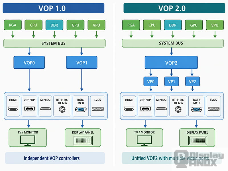
5.1 VOP 1.0
VOP 1.0 is common on platforms such as RK3288, RK3399, and PX30. Multi-display output usually relies on several independent VOP blocks.
Each VOP has its own scanout timing and hardware windows. An interface selects an input such as VOPB or VOPL. Resource ownership is relatively easy to visualize, although sharing resources across VOP blocks is limited.
5.2 VOP 2.0
VOP 2.0 uses a unified display engine with multiple Video Ports:
Shared hardware Window / Plane pool
               ↓
Scaling, composition, CSC, HDR
               ↓
VP0 / VP1 / VP2 / VP3
               ↓
HDMI, DP, eDP, DSI, LVDS, or RGB
The DRM mapping is normally:
Rockchip Window → DRM Plane
Rockchip VP     → DRM CRTC
Multiple VPs can produce independent display timings, while planes are allocated from a shared pool. DCLK, ACLK, AFBC, DSC, HDR, PLLs, and interface routes may also be shared or constrained.
This architecture offers considerable flexibility, but it makes resource conflicts more subtle. A mode may be individually valid and still fail when another display, scaler, AFBC window, or shared clock is active.
6. The Linux Graphics Stack Around DRM
The software stack can be represented as:
Weston / Xorg / SurfaceFlinger / Qt / SDL / modetest
                         ↓
                       libdrm
                         ↓
                      DRM Core
                  ↙               ↘
        GEM / PRIME           KMS / Atomic
                  ↘               ↙
              Rockchip DRM driver
                         ↓
          VOP / VP / Interface / PHY / Panel
libdrm provides convenient userspace wrappers for device opening, resource enumeration, GEM/PRIME operations, dumb buffers, legacy modesetting, Atomic KMS, and event processing.
DRM Core provides the generic objects, ioctls, state handling, and locking. The Rockchip driver implements the hardware-specific VOP, GEM, IOMMU, interface, clock, reset, GRF, PHY, and panel behavior.
When Weston, Xorg, or SurfaceFlinger is running, that compositor normally owns DRM Master. A second process that attempts direct modesetting may fail. Low-level testing should therefore run without a competing compositor, or through the display-management interface provided by the active graphics stack.
7. Display Timing: The First Principle of Panel Bring-Up
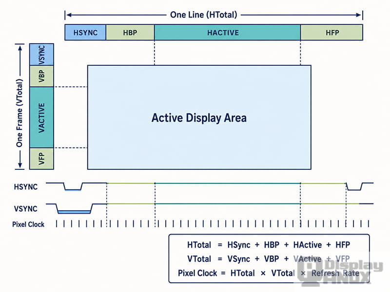
A display interface sends more than the visible pixels. Every line and every frame contains synchronization and blanking intervals.
7.1 Horizontal Timing
htotal = hsync_len + hback_porch + hactive + hfront_porch

hsync_start = hactive + hfront_porch

hsync_end = hactive + hfront_porch + hsync_len
7.2 Vertical Timing
vtotal = vsync_len + vback_porch + vactive + vfront_porch

vsync_start = vactive + vfront_porch

vsync_end = vactive + vfront_porch + vsync_len
7.3 Refresh Rate and Pixel Clock
The approximate relationship is:
refresh rate = pixel clock / (htotal × vtotal)
For a common 1920 × 1080 at 60 Hz CEA timing:
hactive     = 1920
htotal      = 2200
vactive     = 1080
vtotal      = 1125
pixel clock = 148.5 MHz

148,500,000 / (2200 × 1125) = 60 Hz
A panel described as “1920 × 1080” cannot be configured from active resolution alone. The full timing, clock tolerance, polarity, and interface requirements must match the panel datasheet or EDID.
7.4 Polarity and Sampling Edge
Common Device Tree timing properties include:
hsync-active = <0>;
vsync-active = <0>;
de-active = <1>;
pixelclk-active = <0>;
These values define the active levels of HSYNC, VSYNC, and DE, along with the pixel-clock sampling edge. Incorrect settings can cause a black screen, rolling image, edge jitter, random colors, or compatibility problems that appear only on certain panels.
7.5 Fixed Timing and EDID
Modes usually come from one of two sources:
- A panel node supplies fixed timing.
- An HDMI, DP, or eDP sink provides EDID through DDC or AUX.
Fixed timing avoids dependence on EDID but fails when the configured values do not match the panel. EDID is flexible, but it depends on sink power, HPD, DDC or AUX communication, and valid data in the display.
8. Bandwidth: Why a Correct Mode Can Still Produce Corruption
8.1 Image Read Bandwidth
Uncompressed image bandwidth can be estimated as:
image bandwidth = width × height × refresh rate × bytes per pixel
For 1920 × 1080 at 60 Hz using XRGB8888:
1920 × 1080 × 60 × 4 ≈ 497.7 MB/s
This is only the theoretical pixel read rate. A real system must also account for multiple planes, scaling, bus efficiency, DDR contention, AFBC behavior, writeback, RGA, ISP, and VPU traffic.
8.2 Interface Bandwidth
The display interface has a separate bandwidth calculation. For DP or eDP:
effective video bandwidth
<
lane count × link rate × encoding efficiency
HDMI adds TMDS or FRL overhead. MIPI DSI packages pixels into protocol packets. LVDS serializes parallel pixel data across one or two channels. Pixel clock and serial lane rate are related, but they are not interchangeable.
Panox Display’s LCD interface comparison provides additional context for selecting MIPI DSI, LVDS, eDP, RGB, SPI, or other interfaces at the panel level.
8.3 POST_BUF_EMPTY
POST_BUF_EMPTY normally indicates that VOP could not keep its scanout FIFO supplied.
The first checks should cover:
- DDR and AXI bandwidth
- VOP ACLK frequency
- Plane count and scaling load
- AFBC capability and compression behavior
- IOMMU page faults
- Timing with unusually short blanking
- Voltage, clock, or bus-priority instability
Some Rockchip platforms require a higher VOP ACLK for modes above 4K60. The correct frequency must come from the SoC and BSP documentation rather than a generic value.
9. Plane Composition, Scaling, and Color
9.1 Source and Destination Rectangles
Every plane has a source rectangle inside the framebuffer and a destination rectangle on the CRTC:
Source:      SRC_X, SRC_Y, SRC_W, SRC_H
Destination: CRTC_X, CRTC_Y, CRTC_W, CRTC_H
When the dimensions differ, hardware scaling is enabled. The configuration must still satisfy minimum and maximum scaling ratios, alignment rules, YUV chroma-subsampling constraints, maximum input and output widths, and the capabilities of the selected VOP window.
9.2 Z Position and Alpha
zpos defines composition order. Alpha blending also depends on:
- Global alpha
- Per-pixel alpha
- Premultiplied or coverage mode
- Whether the source pixels are already premultiplied
- Whether the selected FourCC format contains alpha
A plane that exists but cannot be seen often has an incorrect Z position, zero alpha, an off-screen destination, or an invalid FB_ID.
9.3 RGB, YUV, and Color-Space Conversion
Video buffers commonly arrive as NV12 or NV16, while the output may be RGB or YUV. Color-space conversion requires a consistent definition of:
- BT.601, BT.709, or BT.2020
- Full or limited range
- RGB or YUV output
- Connector color properties
- HDR transfer function and metadata
Raised black levels, gray-looking video, and incorrect skin tones are often caused by a mismatch in color encoding or quantization range rather than a defective panel.
10. GEM, IOMMU, CMA, Cache Coherency, and Fences
The complete buffer path is:
CPU / GPU / RGA / decoder writes image
        ↓
DMA-BUF or GEM object
        ↓
Producer fence
        ↓
DRM framebuffer: format, pitch, offset, modifier
        ↓
Plane: crop, scale, alpha, Z order
        ↓
IOMMU translates IOVA to physical pages
        ↓
VOP fetches and processes pixels
        ↓
Page-flip event or output fence
        ↓
Interface and panel
10.1 GEM Objects
A GEM object is the kernel representation of a graphics buffer. Its backing memory may come from contiguous CMA, an array of pages mapped through an IOMMU, an imported DMA-BUF, or a platform-specific allocator.
10.2 IOMMU
With an IOMMU enabled, VOP accesses an I/O virtual address rather than requiring one physically contiguous allocation. This improves memory flexibility but makes mapping and lifetime errors visible as page faults.
Useful checks include:
dmesg | grep -Ei 'iommu|page fault|vop|drm'
cat /sys/kernel/debug/dri/0/mm_dump
10.3 Disabling the IOMMU
When the VOP IOMMU is disabled, DRM buffers often come from CMA. CMA must then be large enough for the resolution, pixel format, buffer count, and number of active displays.
Disabling the IOMMU can help isolate an address-mapping problem, but it should not become a permanent fix without a memory-capacity review.
10.4 Cache Coherency and Fences
A shared buffer is safe only when:
- The producer has completed all writes.
- Cache synchronization is correct.
- The scanout device waits for the producer.
- The buffer remains allocated until scanout has finished.
IN_FENCE_FD allows a producer fence to be attached to a plane update. OUT_FENCE_PTR allows the display pipeline to report when it has finished using the committed state.
A fixed delay is not a reliable replacement for proper fence handling.
11. Legacy KMS and Atomic KMS
11.1 Legacy KMS
Typical legacy calls include:
drmModeSetCrtc();
drmModeSetPlane();
drmModePageFlip();
They are easy to understand and remain useful for a minimal bring-up program. Their weakness is that several related objects may be changed in separate operations, creating temporary inconsistent states.
11.2 Atomic KMS
Atomic KMS submits a complete candidate state covering connectors, CRTCs, and planes:
Connector → CRTC_ID
CRTC     → MODE_ID and ACTIVE
Plane    → FB_ID, CRTC_ID, SRC_*, and CRTC_*
The transaction follows this model:
Enumerate objects and properties
        ↓
Build atomic request
        ↓
Run TEST_ONLY
        ↓
atomic_check validates route, timing, format, scaling,
bandwidth, clocks, and shared resources
        ↓
Commit or return an error without changing the display
        ↓
Program hardware at a safe point
        ↓
Generate page-flip event and output fence
11.3 Properties
Atomic state changes are expressed as:
Object ID + Property ID + Value
Properties may be ranges, signed ranges, enumerations, bitmasks, blobs, or references to another object. A display mode is commonly converted into a property blob, and the blob ID is assigned to the CRTC’s MODE_ID.
11.4 TEST_ONLY
A test commit uses:
DRM_MODE_ATOMIC_TEST_ONLY
It validates the proposed route, mode, format, scaling, clock, bandwidth, and shared resources without programming the hardware. This is one of the most useful tools for diagnosing an atomic -EINVAL.
11.5 Nonblocking Commits and Page-Flip Events
DRM_MODE_ATOMIC_NONBLOCK allows the call to return while the hardware update completes asynchronously. DRM_MODE_PAGE_FLIP_EVENT requests an event when the transition is complete.
Applications using both must process events correctly. Otherwise, buffer recycling and frame pacing eventually become unreliable.
12. What Happens Inside an Atomic Commit
12.1 Candidate State
The kernel duplicates the relevant old object states and applies requested property changes to the copies. Hardware remains unchanged during this phase.
12.2 atomic_check
The driver validates each object and any global resource constraints:
Plane check
CRTC check
Encoder and bridge check
Connector check
Shared-resource check
A Rockchip VOP2 driver may calculate plane allocation, scaling capability, bandwidth, DCLK requirements, and interface routing at this stage.
12.3 Commit Sequence
A typical commit tail performs the following work:
- Wait for required fences.
- Disable paths that must be reconfigured.
- Configure PLLs, DCLK, ACLK, PHY, and power resources.
- Program the display mode and interface.
- Configure plane addresses, formats, scaling, and composition.
- Latch the new state at a safe hardware boundary.
- Send a VBlank or page-flip event.
- Release the old state and buffers.
Callback names vary between kernel versions. Source analysis is easier when organized around the five functional stages: validate, disable, configure, enable, and complete.
13. VBlank, Page Flip, and Tear-Free Output
VBlank is the vertical blanking period after the active portion of a frame. A page flip normally changes the scanned framebuffer at a VBlank boundary, preventing the top and bottom of the image from coming from different frames.
Important debugging points include:
- An inactive CRTC does not generate normal VBlank events.
- A missing or blocked interrupt can cause page-flip timeouts.
- An incorrect clock or mode can produce an unexpected refresh rate.
- Variable refresh rate and panel self-refresh change the traditional fixed-VBlank model.
- VBlank debug logging can be extremely verbose and should be enabled only when needed.
14. Rockchip DRM Driver Source-Code Map
A practical reading order starts at the master DRM device and moves toward hardware-specific blocks:
rockchip_drm_drv.c
    ↓
rockchip_drm_vop2.c or rockchip_drm_vop.c
    ↓
HDMI / DP / eDP / DSI / LVDS / RGB driver
    ↓
panel-simple.c or panel-specific driver
    ↓
bridge driver
    ↓
rockchip_drm_gem.c
    ↓
Device Tree bindings and board DTS
Common directories include:
drivers/gpu/drm/rockchip/
drivers/gpu/drm/bridge/analogix/
drivers/gpu/drm/bridge/synopsys/
drivers/gpu/drm/panel/
drivers/phy/rockchip/
| Area | Typical source file | Main reading target |
|---|---|---|
| DRM master | rockchip_drm_drv.c |
Component matching, bind, mode configuration, DMA/IOMMU setup |
| GEM | rockchip_drm_gem.c |
Objects, mmap, PRIME, and IOMMU |
| VOP 1.0 | rockchip_drm_vop.c |
CRTCs, planes, clocks, and register updates |
| VOP 2.0 | rockchip_drm_vop2.c |
VPs, windows, Atomic KMS, scaling, DCLK |
| HDMI | dw_hdmi-rockchip.c, dw-hdmi*.c |
EDID, modes, PHY, audio, and HDCP |
| eDP | analogix_dp-rockchip.c and related files |
AUX, DPCD, HPD, and link training |
| DP | dw-dp.c, cdn-dp-core.c, or BSP equivalent |
Type-C state, HPD, training, and PHY |
| MIPI DSI | dw-mipi-dsi*.c |
Lanes, D-PHY, modes, and command transfer |
| LVDS | rockchip_lvds.c |
Bus format, single/dual channel, and PHY |
| Panel | panel-simple.c or a panel-specific file |
Timing, GPIO, regulators, and delays |
15. Component Framework and Deferred Probe
The Rockchip DRM device is assembled from several independently probed drivers:
VOP/VOP2
Display interface
PHY
Bridge
Panel
Backlight
Clock
Reset
Regulator
GPIO
The initialization flow is:
Drivers probe independently
        ↓
Are all required components ready?
        ├─ No → return -EPROBE_DEFER and retry later
        └─ Yes
             ↓
        Component bind
             ↓
Register CRTC, plane, encoder, and connector
             ↓
Create /dev/dri/cardX
15.1 Interpreting -EPROBE_DEFER and -517
A startup message such as:
Failed to find panel or bridge: -517
is not automatically a final failure. It means that a dependency was not ready at that moment.
The correct questions are:
- Did the driver bind successfully later?
- Did Rockchip DRM finish initialization?
- Was
/dev/dri/cardXcreated? - Did the expected connector appear?
- Does the error continue indefinitely?
If deferred probing never converges, the usual causes are an incorrect panel compatible, incomplete remote-endpoint links, a missing regulator or backlight, the wrong bridge I²C address, a disabled node, or a required driver that was not built.
16. Device Tree Graph Routing
Device Tree graph bindings describe the topology between VOP, an interface controller, a bridge, and a panel.
16.1 port, endpoint, and remote-endpoint
A DSI-to-panel link may be described as:
&dsi0 {
    status = "okay";

    ports {
        port@1 {
            reg = <1>;

            dsi0_out_panel: endpoint {
                remote-endpoint = <&panel_in_dsi0>;
            };
        };
    };
};

panel {
    compatible = "simple-panel-dsi";

    port {
        panel_in_dsi0: endpoint {
            remote-endpoint = <&dsi0_out_panel>;
        };
    };
};
The endpoints should reference each other. A one-sided link can prevent graph traversal or stop the panel or bridge from being discovered.
16.2 Routing a VOP2 VP to an Interface
VOP2 platforms often expose nodes that choose the VP feeding an interface:
&dsi0_in_vp2 {
    status = "okay";
};
Other BSPs use a route_xxx node whose connect property refers to a specific VOP output endpoint. Node names and supported combinations must be taken from the SoC DTSI and its display routing table.
16.3 display-subsystem and the Boot Logo
Rockchip’s display-subsystem often contains route nodes used by U-Boot and the kernel logo path.
Logo continuity depends on:
- The selected route and
connectendpoint - Logo file and mode
- Reserved framebuffer memory
- Compatible U-Boot and kernel timings
- Clock-parent and divider choices
- Consistent power and reset sequencing
A mismatch can cause a black interval, white flash, or corrupted transition between the bootloader and kernel.
17. Panel, Bridge, Backlight, and Power Sequencing
A typical panel sequence is:
Enable panel power
        ↓
Wait for prepare delay
        ↓
Release reset and enable GPIO
        ↓
Initialize DSI, AUX, bridge, or link
        ↓
Start valid VOP video
        ↓
Enable backlight
Shutdown usually follows the reverse order:
Backlight off → video off → interface off → reset/power off
17.1 Panel State Model
The common panel callbacks have these meanings:
| Callback | Typical responsibility |
|---|---|
prepare |
Enable power, release reset, send setup commands, and wait for readiness |
enable |
Start visible output or enable backlight |
disable |
Stop visible output or switch off backlight |
unprepare |
Assert reset and remove power |
Turning on the backlight only after valid video is stable reduces white flashes, residual images, and bright lines during startup.
17.2 Common panel-simple Properties
panel {
    compatible = "simple-panel";
    power-supply = <&vcc_lcd>;
    backlight = <&backlight>;

    enable-gpios = <&gpioX RK_PXX GPIO_ACTIVE_HIGH>;
    reset-gpios = <&gpioY RK_PXX GPIO_ACTIVE_LOW>;

    prepare-delay-ms = <120>;
    enable-delay-ms = <20>;
    disable-delay-ms = <20>;
    unprepare-delay-ms = <120>;
};
These delays are not universal defaults. They must match the panel’s power, reset, video-stability, and backlight requirements.
17.3 Bridge Responsibilities
A complete bridge driver may need to provide:
- Input and output mode validation
- Bus-format negotiation
- Bridge attachment and connector creation
- Power and reset control
- Register initialization
- Atomic enable and disable
- EDID and HPD handling
- Support for multi-bridge chains
18. Display Interfaces in the DRM Pipeline
| Interface | Control path | Video path | Primary debug targets |
|---|---|---|---|
| HDMI | HPD, DDC/EDID, SCDC, HDCP | TMDS or FRL | EDID, DCLK, PHY, cable, sink compatibility |
| DisplayPort | HPD, AUX, DPCD, Type-C state | Main Link | Lane mapping, link training, swing, pre-emphasis |
| eDP | AUX, DPCD, panel timing, HPD | Main Link | Power order, AUX, training, PSR |
| MIPI DSI | DCS or generic commands | D-PHY or C-PHY lanes | Lane rate, mode flags, initialization sequence, TE |
| LVDS | Usually little or no bidirectional control | Differential serialized pixels | JEIDA/VESA, channel order, mapping, swing |
| RGB/TTL | GPIO and timing controls | Parallel pixels, DE, HSYNC, VSYNC | Pinmux, polarity, sampling edge, routing |
19. DP and eDP Bring-Up
A DP or eDP link contains three essential channels:
- Main Link carries display data over one, two, or four lanes.
- AUX carries DPCD, EDID, and configuration traffic.
- HPD reports connection and sink status.
The normal sequence is:
HPD becomes active
        ↓
Read DPCD over AUX
        ↓
Read EDID over AUX/I²C
        ↓
Choose lane count and link rate
        ↓
Run Clock Recovery
        ↓
Run Channel Equalization
        ↓
Send MSA and stream timing
        ↓
Transmit video
19.1 HPD
An active HPD normally indicates that the sink is ready. A design without a physical HPD signal may use a force-HPD setting, but the software then loses genuine connection feedback and depends on a correct fixed power delay.
19.2 AUX and DPCD
DPCD reports capabilities such as maximum link rate, lane count, training features, and link status.
AUX errors commonly come from:
- The panel not being powered
- Incorrect HPD timing
- Reversed or damaged AUX pairs
- An inactive PHY
- Power noise
- A panel-side fault
19.3 Link Training
DisplayPort link training consists mainly of Clock Recovery and Channel Equalization.
When training fails, the investigation should cover DPCD capability reads, lane count, lane mapping, link rate, voltage swing, pre-emphasis, cable or FPC quality, connector impedance, and panel behavior.
Reducing link rate is a useful diagnostic step. It is not a final solution when the product specification requires the original bandwidth.
19.4 Built-In Test Patterns
The available test patterns isolate different portions of the system:
- Panel self-test verifies the panel-side display logic and some power conditions.
- Controller BIST verifies much of the interface controller, PHY, and panel link.
- VP color bars verify the VOP output path while bypassing application buffers.
20. LVDS Bring-Up
Common LVDS bus-format mappings include:
MEDIA_BUS_FMT_RGB666_1X7X3_SPWG   → JEIDA-18
MEDIA_BUS_FMT_RGB888_1X7X4_JEIDA  → JEIDA-24
MEDIA_BUS_FMT_RGB888_1X7X4_SPWG   → VESA-24
20.1 Single-Channel LVDS
A single-channel implementation must confirm panel timing, bus format, selected LVDS controller, VP routing, enable GPIO, power rails, and backlight behavior.
20.2 Dual-Channel LVDS
A dual-channel configuration may contain:
&lvds0 {
    status = "okay";
    dual-channel;
};
Panel endpoints can use properties such as:
dual-lvds-odd-pixels;
dual-lvds-even-pixels;
Reversed odd and even channels commonly produce a sawtooth, interleaved, or blurred image. The channel assignment should be corrected before changing the basic display timing.
20.3 Black-and-White or Incorrect Colors
The main checks are JEIDA versus VESA mapping, 18-bit versus 24-bit operation, media bus format, channel mapping, panel bit depth, enable state, and LVDS PHY electrical levels.
21. MIPI DSI, HDMI, and RGB Engineering Priorities
21.1 MIPI DSI
A practical study order is:
- Video mode versus command mode
- D-PHY lane count, byte clock, and lane rate
- Panel initialization commands
- Burst, sync-pulse, and sync-event modes
- TE, ESD recovery, and suspend/resume
- DSI host attachment to the panel or bridge
A black MIPI display can be caused by the pixel path, initialization sequence, reset timing, lane configuration, backlight, or DRM state. Panox Display’s MIPI DSI display bring-up guide covers these panel-specific stages in more detail.
21.2 HDMI
HDMI bring-up should proceed through HPD, DDC and EDID, mode selection, pixel and TMDS clocks, PHY state, color format, quantization range, audio, and HDCP where required.
An HDMI sink that is detected but remains black has already passed only the first part of the chain. CRTC routing, encoder enable, bridge state, PHY lock, and signal integrity still require confirmation.
21.3 RGB/TTL
RGB is protocol-light but electrically demanding. Its main risks are pinmux, bus width, HSYNC, VSYNC, DE, pixel-clock edge, drive strength, trace length, crosstalk, and timing tolerance.
22. Information Required Before Display Bring-Up
Before source code or Device Tree is changed, the engineering package should contain:
| Required material | Why it matters |
|---|---|
| SoC TRM and display routing table | Defines VOP, VP, interface, clock, and PHY capability |
| Board schematic | Confirms power, reset, HPD, pinmux, lane mapping, and bridge wiring |
| Panel or monitor datasheet | Defines timing, voltage, sequence, bus format, and mechanical interface |
| Interface specification | Defines serial rate, encoding, and control-channel behavior |
| Relevant Rockchip interface guide | Documents BSP-specific nodes and debug methods |
| SDK DTSI and binding YAML | Establishes valid properties and endpoint names |
| Reference-board DTS | Provides a known working topology |
| Bandwidth budget | Confirms that resolution, refresh rate, format, and plane count are feasible |
23. Generic Device Tree Display Template
The following example illustrates structure only. Node names, supplies, GPIOs, timing, bus format, and route selection must be replaced with platform-specific values.
/ {
    backlight: backlight {
        compatible = "pwm-backlight";
        pwms = <&pwmX 0 25000 0>;

        brightness-levels = <0 8 16 32 64 128 192 255>;
        default-brightness-level = <6>;

        power-supply = <&vcc_bl>;
        enable-gpios = <&gpioX RK_PXX GPIO_ACTIVE_HIGH>;
    };

    panel {
        compatible = "simple-panel";
        power-supply = <&vcc_lcd>;
        backlight = <&backlight>;

        enable-gpios = <&gpioY RK_PXX GPIO_ACTIVE_HIGH>;
        reset-gpios = <&gpioZ RK_PXX GPIO_ACTIVE_LOW>;

        prepare-delay-ms = <100>;
        enable-delay-ms = <20>;
        disable-delay-ms = <20>;
        unprepare-delay-ms = <100>;

        bus-format = <MEDIA_BUS_FMT_RGB888_1X24>;

        display-timings {
            native-mode = <&timing0>;

            timing0: timing0 {
                clock-frequency = <74250000>;

                hactive = <1280>;
                vactive = <720>;

                hfront-porch = <110>;
                hsync-len = <40>;
                hback-porch = <220>;

                vfront-porch = <5>;
                vsync-len = <5>;
                vback-porch = <20>;

                hsync-active = <1>;
                vsync-active = <1>;
                de-active = <1>;
                pixelclk-active = <0>;
            };
        };

        port {
            panel_in: endpoint {
                remote-endpoint = <&interface_out>;
            };
        };
    };
};

&display_interface {
    status = "okay";

    ports {
        port@1 {
            reg = <1>;

            interface_out: endpoint {
                remote-endpoint = <&panel_in>;
            };
        };
    };
};

&interface_in_vp0 {
    status = "okay";
};
The mandatory replacements are the node names, regulators, GPIOs, PWM, timing, bus format, interface lane configuration, PHY, HPD behavior, panel compatible, VP route, and power delays.
24. A Seven-Layer Rockchip Display Bring-Up Method
Layer 1: Static Hardware Validation
Before boot, verify all display power rails, ground, reset level, backlight default state, HPD pull state, differential P/N routing, lane order, pinmux, bridge I²C address, required pull-ups, FPC orientation, and connector assembly.
Layer 2: Driver Registration
Search the kernel log:
dmesg | grep -Ei
'drm|vop|display|hdmi|dp|edp|dsi|lvds|panel|bridge|backlight|phy|517'
The expected evidence includes VOP/VOP2 binding, interface binding, panel or bridge binding, convergence of deferred-probe errors, successful DRM initialization, and creation of /dev/dri/cardX.
Layer 3: DRM Objects and Routing
modetest -M rockchip
cat /sys/kernel/debug/dri/0/summary
cat /sys/kernel/debug/dri/0/state
Confirm that the connector exists, connection status is reasonable, modes are available, the expected CRTC and planes exist, possible_crtcs includes the target VP, and a primary plane has been allocated.
Layer 4: Mode and Clock
cat /sys/kernel/debug/clk/clk_summary |
    grep -Ei 'vop|dclk|hdmi|dp|dsi|lvds'
Compare the requested mode with the actual DCLK, PLL parent, divider, interface lane rate, sync polarity, and bus format.
Layer 5: Hardware Test Patterns
Use VP color bars, interface-controller BIST, and panel self-test where available. Each test bypasses a different part of the normal pipeline.
Layer 6: Minimal KMS Output
Use modetest to display a fixed test pattern before starting a compositor, GPU stack, video decoder, or application. This keeps the number of variables small.
Layer 7: Stability Testing
A production-oriented test plan should include at least:
- 100 cold starts
- Warm reboots
- Cable insertion and removal
- Suspend and resume
- Repeated mode switching
- Multi-display operation
- Video and bandwidth stress
- High- and low-temperature operation
- Long-duration testing
25. Practical modetest Workflow
25.1 Enumerating Resources
modetest -M rockchip
A useful reading order is:
Connectors → Modes → Encoders → CRTCs → Planes → Properties
25.2 Displaying an SMPTE Pattern
modetest -M rockchip
    -s <connector_id>@<crtc_id>:<mode>
Example:
modetest -M rockchip -s 156@71:1920x1080
Object IDs must come from the active system. They are not stable across platforms or necessarily across boots.
25.3 Testing an Overlay Plane
Exact options vary between libdrm versions, so modetest -h should be checked first. A useful test should select an overlay plane, use ARGB or NV12, set different source and destination rectangles, and exercise scaling, Z position, and alpha.
25.4 Inspecting Atomic Properties
Important properties include:
CRTC_ID
MODE_ID
ACTIVE
FB_ID
SRC_X/Y/W/H
CRTC_X/Y/W/H
zpos
alpha
rotation
COLOR_ENCODING
COLOR_RANGE
Content Protection
26. Experiment One: Enumerate DRM Resources
The following program opens the Rockchip DRM device when possible, falls back to scanning KMS-capable card nodes, and prints the available CRTCs, connectors, encoders, and modes.
#include <errno.h>
#include <fcntl.h>
#include <stdio.h>
#include <stdlib.h>
#include <string.h>
#include <unistd.h>

#include <xf86drm.h>
#include <xf86drmMode.h>

static int open_rockchip_drm(void)
{
    int fd = drmOpen("rockchip", NULL);

    if (fd >= 0)
        return fd;

    for (int i = 0; i < 16; ++i) {
        char path[64];

        snprintf(path, sizeof(path), "/dev/dri/card%d", i);
        fd = open(path, O_RDWR | O_CLOEXEC);

        if (fd < 0)
            continue;

        if (drmIsKMS(fd))
            return fd;

        close(fd);
    }

    return -1;
}

int main(void)
{
    int fd = open_rockchip_drm();

    if (fd < 0) {
        fprintf(stderr, "No KMS device found
");
        return 1;
    }

    drmModeRes *res = drmModeGetResources(fd);

    if (!res) {
        fprintf(stderr, "drmModeGetResources: %s
",
                strerror(errno));
        close(fd);
        return 1;
    }

    printf("crtcs=%d connectors=%d encoders=%d
",
           res->count_crtcs,
           res->count_connectors,
           res->count_encoders);

    for (int i = 0; i < res->count_connectors; ++i) {
        drmModeConnector *connector =
            drmModeGetConnector(fd, res->connectors[i]);

        if (!connector)
            continue;

        printf("connector id=%u state=%d modes=%d encoder=%u
",
               connector->connector_id,
               connector->connection,
               connector->count_modes,
               connector->encoder_id);

        for (int m = 0; m < connector->count_modes; ++m) {
            drmModeModeInfo *mode = &connector->modes[m];

            printf("  %s %dx%d clock=%d kHz
",
                   mode->name,
                   mode->hdisplay,
                   mode->vdisplay,
                   mode->clock);
        }

        drmModeFreeConnector(connector);
    }

    drmModeFreeResources(res);
    close(fd);
    return 0;
}
A typical cross-compile command is:
$CC drm_enum.c -o drm_enum
    $(pkg-config --cflags --libs libdrm)
27. Experiment Two: Display a Solid Color with a Dumb Buffer
The minimal flow is:
Open DRM device
    ↓
Select a connected connector
    ↓
Select a mode and compatible CRTC
    ↓
Create dumb buffer
    ↓
Create framebuffer
    ↓
Map buffer into userspace
    ↓
Fill pixels
    ↓
Set CRTC
    ↓
Observe the display
    ↓
Restore old state and release resources
A dumb buffer can be created with:
struct drm_mode_create_dumb create = {
    .width = width,
    .height = height,
    .bpp = 32,
};

ioctl(fd, DRM_IOCTL_MODE_CREATE_DUMB, &create);
The returned values include handle, pitch, and size.
A framebuffer can then be created:
uint32_t handles[4] = { create.handle };
uint32_t pitches[4] = { create.pitch };
uint32_t offsets[4] = { 0 };

drmModeAddFB2(fd,
              width,
              height,
              DRM_FORMAT_XRGB8888,
              handles,
              pitches,
              offsets,
              &fb_id,
              0);
The display mode is applied with:
drmModeSetCrtc(fd,
               crtc_id,
               fb_id,
               0,
               0,
               &connector_id,
               1,
               &mode);
This experiment bypasses the GPU, compositor, and decoder. It directly tests the DRM device, connector-to-CRTC route, mode, GEM allocation, primary plane, VOP, and interface.
28. Experiment Three: Overlay Planes and DMA-BUF
28.1 Overlay Plane Test
A complete overlay test should:
- Enumerate all planes.
- Check each plane’s
possible_crtcs. - Inspect the supported formats.
- Create an ARGB or NV12 framebuffer.
- Set source and destination rectangles.
- Configure Z position and alpha.
- run an Atomic
TEST_ONLYrequest. - Commit the validated state.
28.2 Importing DMA-BUF
uint32_t handle;

drmPrimeFDToHandle(drm_fd, dma_buf_fd, &handle);
For a multi-plane format, each plane must have the correct handle, pitch, offset, and modifier.
28.3 Fence Handling
For continuous video:
- The decoder’s completion fence is assigned to
IN_FENCE_FD. - DRM returns an output fence through
OUT_FENCE_PTR. - The producer reuses the buffer only after the display fence has completed.
- Frame lifetime must not be estimated with a fixed sleep.
29. Rockchip DRM Debugging Toolbox
29.1 Mounting debugfs
mount -t debugfs none /sys/kernel/debug
The kernel requires:
CONFIG_DEBUG_FS=y
29.2 Display Summary
cat /sys/kernel/debug/dri/0/summary
The summary should be examined for the active VP or CRTC, connector, mode, DCLK, refresh rate, plane or window, pixel format, pitch, buffer address, source and destination rectangles, HDR or CSC state, and ACTIVE or DISABLED status.
29.3 Atomic State
cat /sys/kernel/debug/dri/0/state
This shows DRM object IDs, properties, and current binding relationships.
29.4 VOP Registers
Linux 6.1 and newer Rockchip BSPs commonly expose:
cat /sys/kernel/debug/dri/0/active_regs
cat /sys/kernel/debug/dri/0/regs
Older BSPs may require vop2_dump.sh or a platform-specific register-dump tool.
29.5 Dumping the Current Buffer
Some BSPs require:
CONFIG_ROCKCHIP_DRM_DEBUG=y
A VOP 1.0 node may look like:
echo dump >
/sys/kernel/debug/dri/0/ff900000.vop/vop_dump/dump
A VOP2 node may look like:
echo dump >
/sys/kernel/debug/dri/0/video_port0/dump
The actual path must be taken from the active debugfs tree.
29.6 VP Color Bars
echo 1 >
/sys/kernel/debug/dri/0/video_port0/color_bar

echo 2 >
/sys/kernel/debug/dri/0/video_port0/color_bar

echo 0 >
/sys/kernel/debug/dri/0/video_port0/color_bar
Commonly, 1 enables horizontal bars, 2 enables vertical bars, and 0 disables the pattern. BSP behavior should be verified before relying on those values.
29.7 DRM Debug Categories
echo 0x10 > /sys/module/drm/parameters/debug
echo 0xff > /sys/module/drm/parameters/debug
Common category bits include:
| Bit | Value | Category |
|---|---|---|
| 0 | 0x01 |
CORE |
| 1 | 0x02 |
DRIVER |
| 2 | 0x04 |
KMS |
| 3 | 0x08 |
PRIME |
| 4 | 0x10 |
ATOMIC |
| 5 | 0x20 |
VBL |
| 7 | 0x80 |
LEASE |
| 8 | 0x100 |
DP |
VBlank logging produces a large volume of output and should not remain enabled unnecessarily.
29.8 Clock, GPIO, and GEM State
cat /sys/kernel/debug/clk/clk_summary
cat /sys/kernel/debug/clk/clk_summary |
    grep -Ei 'vop|dclk'

cat /sys/kernel/debug/gpio
cat /sys/kernel/debug/dri/0/mm_dump
29.9 Forcing Connector Status
Some BSPs support:
echo off > /sys/class/drm/card0-LVDS-1/status
echo on  > /sys/class/drm/card0-LVDS-1/status
This interface is not available in every mainline or BSP kernel and must be confirmed on the target system.
29.10 EDID and Interface State
cat /sys/class/drm/card0-HDMI-A-1/edid
    > /tmp/edid.bin

edid-decode /tmp/edid.bin

cat /sys/kernel/debug/dw-hdmi/status
DP and eDP debugging should also include DPCD, AUX, and link-training logs.
30. Isolating a Display Fault with Test Patterns
Testing the whole chain at once usually produces ambiguous results. Each diagnostic source should bypass a deliberate section of the pipeline.
| Test | What it bypasses | What a correct result suggests |
|---|---|---|
| Dump framebuffer | Display output path | The source image and buffer layout are valid |
| VP color bars | Application and normal buffer path | VOP output and the downstream path are operating |
| Controller BIST | VOP and upstream composition | Controller, PHY, and panel path are operating |
| Panel self-test | SoC video output | Panel power and internal display logic are operating |
No single visual test proves the entire system. The result should be combined with clock, power, register, and state evidence.
31. Rockchip Black Screen Diagnostic Tree
A practical decision tree is:
Black screen
    ↓
Is the backlight on?
    ├─ No → Check PWM, GPIO, power, polarity, and panel sequence
    └─ Yes
         ↓
Does the connector exist and report the expected state?
    ├─ No → Check driver bind, graph, HPD, EDID, panel, and bridge
    └─ Yes
         ↓
Are mode and DCLK correct in the DRM summary?
    ├─ No → Check timing, polarity, bus format, PLL, and lane rate
    └─ Yes
         ↓
Does a VP test pattern display correctly?
    ├─ Yes → Investigate plane, framebuffer, Atomic KMS, and application
    └─ No  → Investigate interface, PHY, cable, power, and panel
31.1 Backlight Off
The first checks are PWM output, enable GPIO, backlight supply, PWM polarity, brightness-levels, default brightness index, panel enable timing, and pin conflicts.
31.2 Backlight On but No Image
Verify, in order:
- Connector status
- Available mode
- CRTC
ACTIVE - Plane
FB_ID - VP color bars
- Interface-controller state
- PHY state
- Panel timing and reset
31.3 Connector Missing
Common causes include a disabled interface node, missing kernel driver, failed component bind, incomplete Device Tree graph, unregistered bridge or panel, and an incorrect compatible.
31.4 Connector Disconnected
For HDMI, DP, and eDP, check HPD, DDC or AUX, cable, sink power, force-HPD configuration, and Type-C Alternate Mode state.
A fixed panel may always report connected; this depends on the driver.
31.5 Empty Mode List
An empty mode list usually points to failed EDID access, missing fixed timing, a bridge that did not report modes, rejection by mode_valid, or a clock and bandwidth limit.
32. Distorted Images, Flicker, and Color Errors
| Symptom | First areas to check |
|---|---|
| Entire image shifted or rolling | Porches, sync width, pixel clock, polarity, and panel active-area definition |
| Fixed bands or periodic corruption | Pitch, FourCC, modifier, DDR bandwidth, FIFO underflow, and scaling |
| Random dots affected by cable position | PHY signal quality, impedance, lane mapping, P/N polarity, swing, and grounding |
| Black-and-white or swapped colors | RGB/BGR, JEIDA/VESA, bus format, CSC, quantization range, and panel bit depth |
| Only one plane is wrong | Plane format, source/destination rectangles, alpha, Z order, DMA-BUF layout, IOMMU, and fences |
| Intermittent black screen | Hot-plug state, suspend sequence, IOMMU mappings, clocks, and resource contention |
32.1 Overall Image Displacement
Check HFP, HBP, HSYNC, VFP, VBP, VSYNC, pixel clock, synchronization polarity, and the panel’s definition of the active area.
32.2 Fixed Stripes or Repeating Corruption
Prioritize pitch, format, modifier, DDR/VOP bandwidth, FIFO underflow, and scaling constraints.
32.3 Random Noise
Noise that changes with the cable, FPC, or connector position usually points to the electrical path: differential impedance, P/N orientation, lane mapping, swing, pre-emphasis, grounding, or power noise.
32.4 Incorrect Color
Check RGB/BGR ordering, bus format, LVDS JEIDA/VESA mapping, YUV color encoding, full or limited range, CSC configuration, and panel bit depth.
32.5 One Faulty Plane
If other planes display correctly, the CRTC and output interface are probably operational. The investigation can focus on the affected plane’s FourCC, pitch, modifier, source and destination rectangles, alpha, Z position, DMA-BUF layout, IOMMU mapping, fence state, and hardware-window capability.
33. Display Clock Failures
33.1 DCLK
DCLK defines the scanout pixel clock. Compare:
- The clock required by the mode
- The value requested by the driver
- The value reported by
clk_summary - The selected PLL parent
- The divider error
DP and HDMI can be sensitive to standard clock accuracy. Even a small difference can matter when a sink has a narrow tolerance or another clock relationship is incorrect.
33.2 ACLK
ACLK affects the ability of VOP to read from DDR. A correct DCLK does not guarantee sufficient memory bandwidth. High resolution, multiple planes, and heavy scaling require ACLK and DDR frequency to be checked independently.
33.3 Bootloader-to-Kernel Clock Changes
U-Boot and the kernel may use different PLL parents, dividers, power-domain states, and clock policies. This can produce a flash or black interval during logo handover.
clk_ignore_unused can help diagnose an incorrectly described dependency, but it should not replace a correct clock tree in production.
34. IOMMU and Memory Failures
34.1 IOMMU Page Fault
Common causes include:
- A buffer was released while still being scanned.
- Pitch or offset extends beyond the mapped allocation.
- DMA-BUF import or attachment failed.
- Address width or scatter-gather handling is wrong.
- Suspend/resume did not restore mappings correctly.
34.2 GEM Allocation Failure
Check CMA capacity, resolution, bit depth, buffer count, number of displays, multi-plane formats, memory fragmentation, and whether the IOMMU has been disabled.
34.3 Buffer Dump as Evidence
If the dumped framebuffer is already wrong, the investigation should move toward the application, decoder, RGA, format, pitch, or memory producer.
If the dump is correct but the panel image is wrong, attention should move toward VOP processing, the interface, PHY, cabling, or panel.
35. Hot Plug, Suspend/Resume, and Intermittent Failures
35.1 Hot Plug
A complete hot-plug investigation includes:
- HPD interrupt behavior
- Connector state transitions
- EDID cache invalidation
- Link-training retries
- Compositor reconfiguration
- HDCP state
- Whether an old buffer remains active after disconnect
35.2 Suspend and Resume
A robust suspend sequence normally stops commits, disables the backlight, stops the video stream, disables the interface and PHY, saves or releases state, and then enters low power.
Resume restores power and clocks, reinitializes or retrains the link, restores mode and plane state, and enables the backlight only after stable video returns.
Incorrect ordering can cause a wake-up black screen, white flash, link-training failure, IOMMU fault, VBlank timeout, or a panel that remains in reset.
35.3 Intermittent Failure Method
Intermittent problems require disciplined recording. The useful data includes the reproduction rate, temperature, power state, number of plug or suspend cycles, last known Atomic KMS state, clock and GPIO state, HPD state, and the first abnormal log entry.
Later errors are often consequences of the initial fault.
36. Multi-Display Output
36.1 Independent Displays
Each VP drives a separate mode and image. Constraints include VP-to-interface routing, plane allocation, DCLK resources, aggregate memory bandwidth, and shared PHY, PLL, DSC, or HDR blocks.
36.2 Connector Mirror
One VP drives several connectors with the same image. The modes must normally be identical or compatible, and the BSP must support the intended mirror route.
36.3 Connector Split
One wide image is divided between two interfaces or panels. The design must account for the left and right regions, synchronized timing, pixel order, dual-LVDS odd/even mapping, and the physical arrangement of bridges and panels.
37. One-Command Rockchip DRM Diagnostic Collection
The following script gathers the core state needed for a display investigation. Paths and permissions may require BSP-specific changes.
#!/bin/sh

OUT=${1:-/tmp/drm_diag}
mkdir -p "$OUT"

mountpoint -q /sys/kernel/debug ||
    mount -t debugfs none /sys/kernel/debug

{
    date
    uname -a
    cat /proc/cmdline
} > "$OUT/system.txt" 2>&1

ls -l /dev/dri > "$OUT/dri_nodes.txt" 2>&1
modetest -M rockchip > "$OUT/modetest.txt" 2>&1

dmesg > "$OUT/dmesg.txt" 2>&1
cat /sys/kernel/debug/clk/clk_summary
    > "$OUT/clk_summary.txt" 2>&1
cat /sys/kernel/debug/gpio
    > "$OUT/gpio.txt" 2>&1

for d in /sys/kernel/debug/dri/*; do
    [ -d "$d" ] || continue
    n=$(basename "$d")

    for f in name summary state active_regs regs mm_dump; do
        [ -r "$d/$f" ] &&
            cat "$d/$f" > "$OUT/dri_${n}_${f}.txt" 2>&1
    done
done

for c in /sys/class/drm/card*-*; do
    [ -d "$c" ] || continue
    n=$(basename "$c")

    [ -r "$c/status" ] &&
        cat "$c/status" > "$OUT/${n}_status.txt"

    [ -r "$c/modes" ] &&
        cat "$c/modes" > "$OUT/${n}_modes.txt"

    [ -r "$c/edid" ] &&
        cat "$c/edid" > "$OUT/${n}_edid.bin"
done

tar czf "${OUT}.tar.gz"
    -C "$(dirname "$OUT")" "$(basename "$OUT")"

echo "Saved: ${OUT}.tar.gz"
The kernel log should not be cleared before collection. The first abnormal event is often the most valuable evidence.
38. Tracing One Atomic Commit Through the Source
A productive source-reading path is:
- Start with
drmModeAtomicCommit()in userspace. - Follow the DRM ioctl into the kernel.
- Find the generic Atomic KMS helper.
- Observe object-state acquisition and property parsing.
- Enter the Rockchip
atomic_checkimplementation. - Follow VOP2 plane and CRTC validation.
- Follow encoder and bridge validation.
- Trace the commit tail.
- Identify register writes and
cfg_done. - Follow the VBlank event and release of old buffers.
For each function, five questions keep the investigation focused:
- What state enters this function?
- What constraint does it validate?
- Does it modify software state or hardware registers?
- What error does it return?
- Which function or stage runs next?
When a kernel message is found, the source should be searched for the exact text:
grep -R "log message"
    -n drivers/gpu/drm drivers/phy
The condition surrounding the message is usually more informative than the message itself.
39. An Eight-Week DRM/KMS Learning Plan
| Week | Theory target | Practical target |
|---|---|---|
| 1 | Timing, pixel formats, bandwidth, and display interfaces | Calculate three modes and bandwidth budgets |
| 2 | DRM object relationships | Enumerate resources and draw the active topology |
| 3 | GEM, dumb buffers, and framebuffers | Display a solid color |
| 4 | Planes, scaling, alpha, and Z position | Run an overlay-plane experiment |
| 5 | Atomic KMS, properties, VBlank, and fences | Use TEST_ONLY and page-flip events |
| 6 | Rockchip VOP/VOP2, components, and Device Tree | Modify one known display route |
| 7 | One physical interface in depth | Use test patterns and interface-specific diagnostics |
| 8 | DMA-BUF, multi-display, performance, and suspend | Run zero-copy video and stability tests |
40. Four Useful DRM/KMS Test Programs
40.1 Resource Enumerator
It should report DRM devices, connectors, modes, encoders, CRTCs, planes, formats, and properties.
40.2 Dumb-Buffer Test
It should create an XRGB8888 buffer, set a mode, display a solid color, save and restore the original CRTC state, and release every resource correctly.
40.3 Overlay-Plane Test
It should exercise ARGB and NV12 planes, scaling, alpha, Z position, and supported format constraints.
40.4 DMA-BUF and Atomic KMS Test
It should import a V4L2 or MPP buffer, create a framebuffer with the correct modifier, use input and output fences, submit nonblocking commits, handle page-flip events, and sustain 30 or 60 frames per second.
41. Rockchip Display Bring-Up Acceptance Checklist
Driver and DRM Objects
- Rockchip DRM completes initialization.
- VOP/VP, interface, bridge, and panel all bind.
- Connector, CRTC, and planes enumerate correctly.
possible_crtcsmatches the intended path.- Mode and refresh rate are correct.
Hardware and Timing
- All power rails meet the panel specification.
- Reset, enable, and backlight sequencing is correct.
- DCLK and interface lane rate are correct.
- Polarity, sampling edge, and bus format are correct.
- HPD, EDID, DDC, or AUX is operational.
- PHY signal quality meets the interface requirement.
Display Functions
- VP color bars display correctly.
modetestdisplays its test pattern.- RGB and YUV planes work.
- Scaling, alpha, and Z position work.
- Multi-display routing works.
- DMA-BUF zero-copy output is stable.
Stability
- Cold boot and warm reboot pass.
- Suspend and resume pass.
- Hot plug passes.
- Mode switching passes.
- High-bandwidth stress passes.
- Long-duration testing passes.
- No IOMMU faults, VBlank timeouts, or FIFO underflows remain.
42. Panox Display’s View of Rockchip Display Integration
A successful Rockchip display product begins with matching the panel and host before driver work starts. Resolution, refresh rate, pixel format, MIPI lane count, eDP or DP link capability, LVDS mapping, timing tolerance, FPC orientation, connector choice, backlight requirements, and power sequencing all affect the software architecture.
Panox Display supports LCD, AMOLED, OLED, and Micro OLED projects with panel selection, datasheet review, interface matching, connector information, timing and initialization guidance, and evaluation of direct-interface or bridge-board approaches.
When a Rockchip design cannot connect directly to the selected panel, Panox Display’s custom display controller and driver boards can provide HDMI or USB Type-C input with MIPI DSI, RGB, LVDS, or eDP output. This approach can reduce prototype risk while the final SoC carrier board and native Linux display path are still under development.
The engineering principle remains the same in either case: panel selection, electrical design, bandwidth, software routing, and validation must be planned as one display system.
Frequently Asked Questions
What is the difference between Rockchip VOP and VOP2?
VOP 1.0 platforms normally use multiple independent VOP blocks, each with its own timing generator and windows. VOP2 uses one shared display engine with a pool of windows and multiple Video Ports. Each VP normally maps to a DRM CRTC.
What does a DRM CRTC correspond to on RK3588?
A DRM CRTC normally corresponds to one VOP2 Video Port, such as VP0, VP1, VP2, or VP3.
Why is a Rockchip display black even when the backlight is on?
The backlight is independent of the pixel pipeline. The fault may still be in the connector, mode, CRTC, plane, framebuffer, VOP route, interface controller, PHY, timing, reset, or panel initialization.
Is -EPROBE_DEFER or -517 always an error?
No. It often means a dependency has not probed yet. It becomes a real problem when the driver never binds successfully and the expected DRM objects do not appear.
Why does modetest fail with -EINVAL?
The requested atomic state violates a constraint. Common causes include an invalid route, unsupported plane format, illegal scaling ratio, missing property, incompatible mode, shared-resource conflict, or insufficient bandwidth. A TEST_ONLY commit and DRM atomic logging can identify the failing stage.
Why does the image look correct in a buffer dump but wrong on the panel?
A correct dump shifts the investigation downstream toward VOP format handling, scaling, CSC, interface timing, PHY signal integrity, lane mapping, and panel configuration.
What causes POST_BUF_EMPTY on Rockchip?
The message usually indicates VOP FIFO underflow. DDR bandwidth, VOP ACLK, plane count, scaling, AFBC, IOMMU faults, and competing memory traffic should be checked.
Can a MIPI, LVDS, or eDP panel connect directly to HDMI?
No. These are different electrical and protocol interfaces. A compatible bridge or controller board is required unless the SoC provides the panel’s native interface.
Why does direct DRM testing fail while the desktop is running?
The compositor usually owns DRM Master. Direct modesetting should be performed without the competing compositor or through an interface designed for the active desktop environment.
What is the fastest reliable method for debugging a Rockchip black screen?
The fastest method is layered isolation: verify power and reset, confirm driver binding, inspect connector and mode state, validate DCLK, display a VP color bar, test the interface controller, and then divide the remaining fault between the upstream buffer path and downstream PHY or panel path.
Appendix A: Command Reference
# Enumerate DRM resources
modetest -M rockchip

# Current display topology and state
cat /sys/kernel/debug/dri/0/summary
cat /sys/kernel/debug/dri/0/state

# VOP registers
cat /sys/kernel/debug/dri/0/active_regs
cat /sys/kernel/debug/dri/0/regs

# Clocks and GPIO
cat /sys/kernel/debug/clk/clk_summary
cat /sys/kernel/debug/gpio

# GEM and IOMMU
cat /sys/kernel/debug/dri/0/mm_dump

# Atomic DRM logging
echo 0x10 > /sys/module/drm/parameters/debug
dmesg -w

# VP color bars
echo 1 > /sys/kernel/debug/dri/0/video_port0/color_bar
echo 0 > /sys/kernel/debug/dri/0/video_port0/color_bar

# EDID
cat /sys/class/drm/card0-HDMI-A-1/edid
    > /tmp/edid.bin
edid-decode /tmp/edid.bin

# Relevant kernel messages
dmesg | grep -Ei
'drm|vop|dclk|hdmi|dp|edp|dsi|lvds|panel|bridge|phy|iommu|fault|timeout|error'
Appendix B: Common Errors and Their Meaning
| Symptom or message | Direct meaning | First checks |
|---|---|---|
-EPROBE_DEFER / -517 |
A dependency is not ready | Final bind result, graph, panel, regulator, and bridge |
Connector disconnected |
Sink not detected | HPD, cable, power, and Type-C state |
| Empty mode list | No usable mode | EDID, fixed timing, bridge modes, and mode_valid |
Atomic -EINVAL |
Candidate state violates a constraint | Properties, route, format, scaling, clocks, and bandwidth |
POST_BUF_EMPTY |
VOP FIFO underflow | DDR, ACLK, planes, scaling, AFBC, and IOMMU |
| IOMMU page fault | VOP accessed an invalid IOVA | Lifetime, pitch, offset, mapping, and resume state |
| VBlank timeout | Expected CRTC interrupt did not arrive | Mode, IRQ, clock, and CRTC ACTIVE |
| Link training failed | DP/eDP Main Link was not established | DPCD, lanes, rate, PHY, and cable |
| AUX error | DP/eDP control communication failed | Power order, HPD, AUX wiring, and sink |
| Dual-LVDS sawtooth image | Odd/even channel order may be reversed | Odd/even properties and physical lane order |
| Backlight on, no image | Light source works but pixel path does not | CRTC, plane, interface, PHY, and timing |
Appendix C: Display Debug Record Template
Platform / SoC:
Kernel and BSP:
Display interface:
Panel or monitor model:
Target mode:
Reproduction rate:
First affected version:

Observed symptom:

Display route:
Plane → CRTC/VP → Encoder/Bridge → Connector → Panel

Confirmed facts:
1.
2.
3.

First relevant log:

DRM summary/state:

Clock, GPIO, EDID, or DPCD evidence:

Self-test results:
- Buffer dump:
- VP color bar:
- Controller BIST:
- Panel self-test:

Controlled comparison:

Most likely root cause:

Validation after the fix: