


![]()
In the rapidly evolving world of display technology, Micro OLED (also known as OLEDoS or Silicon-based OLED) stands out as a game-changer. As the preferred display standard for next-generation devices like the Apple Vision Pro, Micro OLED is redefining visual immersion. This guide explores the structure, manufacturing process, and key differences between Micro OLED and traditional AMOLED, helping you understand why this technology is the future of Augmented and Virtual Reality (AR/VR).
What is Micro OLED (OLEDoS)?
Micro OLED represents a significant leap forward from traditional organic light-emitting diode technology. Unlike conventional OLEDs that use a glass substrate, Micro OLED utilizes a single-crystal silicon wafer as the backplane. By leveraging CMOS (Complementary Metal-Oxide-Semiconductor) process technology, manufacturers can integrate the driver backplane directly into the silicon chip.
This shift from glass to silicon allows for incredible miniaturization. The pixel size in Micro OLEDs can be reduced to approximately 1/10th of the size of traditional OLED pixels, resulting in ultra-high resolution and pixel density (PPI) that glass-based displays simply cannot match. This precision makes Micro OLED the ideal candidate for "near-eye" display applications where clarity is paramount.
Related: Micro LED vs OLED for Near-Eye Displays: Where Micro OLED Fits Best in AI Glasses & XR
The Driving Force Behind XR
The technology is currently seeing explosive interest in the Virtual Reality (VR) and Augmented Reality (AR) sectors. With the launch of high-end headsets like the Apple Vision Pro, Silicon-based OLED is becoming the standard for delivering immersive, realistic interactive experiences. In the AR space, Micro OLED paired with "Birdbath" optical designs has already become the mainstream solution for consumer-grade AR glasses, with demand expected to climb as shipment volumes grow.
Related: AR display panel
The Anatomy of a Micro OLED Display
The superior performance of Micro OLED comes from its unique structure, which fuses semiconductor manufacturing with display technology. The device consists of two primary components: the Drive Backplane and the OLED Front-End.
-
The Drive Backplane: Using CMOS technology, different functional modules of the driver chip are integrated directly onto a single-crystal silicon chip. This simplifies external wiring, reduces weight, and enables the fine-pixel control necessary for high-definition viewing.
-
The OLED Front-End: This is the light-emitting section, deposited directly onto the silicon substrate. It consists of a pixel anode layer, an organic light-emitting layer, a cathode layer, and a color filter.
How It Works
The light generation process is a marvel of physics. The anode and cathode form a circuit. When an external electric field is applied to the organic light-emitting layer (which includes hole injection/transport layers and electron transport/injection layers), holes and electrons move toward each other to form "excitons". These excitons undergo relaxation and diffusion to release energy as light. Finally, a Color Filter (CF) processes this white light to produce the Red, Green, and Blue (RGB) primaries, allowing for the creation of any desired color.
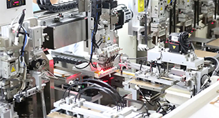
The 5-Step Manufacturing Process
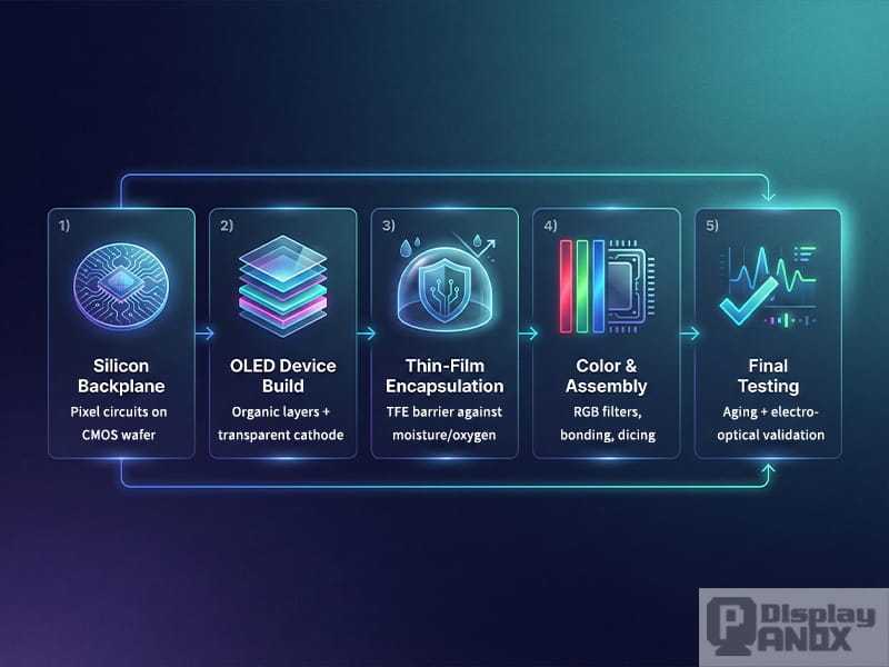
5-Step Micro OLED Manufacturing Process
Manufacturing Micro OLEDs is a complex convergence of semiconductor and panel fabrication techniques. The process is generally divided into five critical stages:
-
Silicon Backplane Fabrication: This requires close collaboration between IC design houses and panel manufacturers. The pixel circuits are designed and then integrated/manufactured by a wafer foundry.
-
OLED Device Fabrication: Once the backplane is ready, the organic light-emitting diode is built. This involves preparing the metal anode, followed by the precise evaporation of the hole injection, transport, emitting, and electron transport layers, concluding with a transparent cathode.
-
Thin-Film Encapsulation (TFE): To protect the organic materials from water and oxygen (to which they are highly sensitive), a dense thin film is applied using PECVD or ALD processes.
-
Colorization & Module Assembly: Using coating, exposure, and development processes, the RGB color filters are created and bonded with a glass cover. The wafer is then diced into individual chips.
-
Final Testing: The chips undergo aging, photoelectric performance testing, and binding with the display system to form a complete module.
Micro OLED vs. Traditional AMOLED: What’s the Difference?
For industry professionals, understanding the distinction between standard AMOLED and Micro OLED is vital. While both are Active Matrix (AM) driven, their manufacturing barriers and performance capabilities differ significantly.
Related: What is AM-OLED Display
Comparison: Micro OLED vs. Traditional AMOLED
|
The "RGB" Challenge
Traditional AMOLEDs typically use a "Fine Metal Mask" (FMM) to evaporate Red, Green, and Blue materials separately, allowing for independent light emission. However, the standard FMM technology used for smartphones cannot meet the microscopic precision required for Micro OLEDs. Consequently, the mainstream Micro OLED solution currently uses WOLED + Color Filter. While this sacrifices some brightness compared to native RGB, it is the most viable mass-production method today. Companies like eMagin and Sunic System are actively researching direct RGB patterning (dPd) and Ultra-High Resolution Masks (UHM) to overcome this bottleneck.
Supply Chain and Market Landscape
The Micro OLED industry relies on a global ecosystem.
-
Upstream: Suppliers of silicon wafers, metal anodes, and organic luminescent materials. Equipment for evaporation and photolithography is critical here, determining yield and precision.
-
Midstream (Panel Manufacturing): Historically dominated by US and European firms like eMagin and Microoled, and Japanese giants like Sony. However, Chinese enterprises are aggressively entering the market, expanding capacity for consumer-level panels.
-
Downstream (Applications): While currently focused on AR/VR headsets, applications are expanding into industrial security, medical devices, electronic viewfinders (EVF), and thermal imaging.
Challenges and Future Outlook
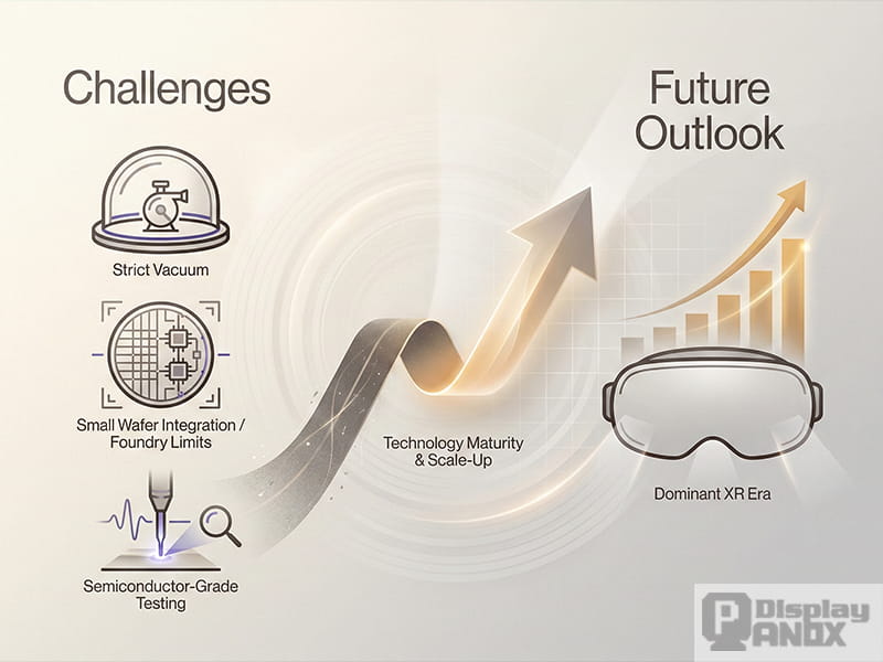
Micro OLED Challenges and Future Outlook
Despite its promise, Micro OLED manufacturing is not without challenges. The process is technically demanding; organic materials require strict vacuum environments, and the integration of circuits on small wafers tests the limits of foundry capabilities. Furthermore, as display refresh rates and resolutions increase, the requirements for testing equipment have skyrocketed, pushing suppliers to develop testing solutions that rival semiconductor-grade inspection tools.
However, the trajectory is clear. As production capacity expands and technology matures, Micro OLED is set to become the dominant display solution for the XR era, offering the high brightness, contrast, and resolution that the metaverse demands.
Learn more: Sony Micro OLED (OLEDoS) Explained: Technology, Applications, and AR/VR Advantages
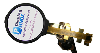
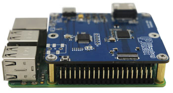
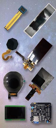
Looking for Micro OLED solutions for your next project?
Explore our product catalog to see how our high-performance Micro OLED modules can elevate your optical designs.