


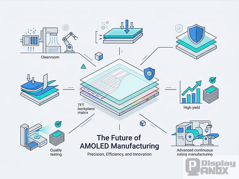
Active-Matrix Organic Light-Emitting Diode (AMOLED) technology represents the pinnacle of modern display engineering. Behind the vibrant colors and infinite contrast ratios of today's smartphones, wearables, and AR/VR headsets lies a highly complex, multi-stage manufacturing process.
The entire manufacturing workflow is a massive system engineering feat involving hundreds of precise steps, broadly categorized into five core stages: Substrate Preparation, TFT Backplane Fabrication, Organic Layer Evaporation, Encapsulation, and Module Assembly.
Here is an in-depth look at how AMOLED displays are made, the technological barriers manufacturers face, and the latest trends shaping the industry in 2026.
Learn more:The Ultimate AMOLED Display Price Guide & Cost Factors
The 5 Core Stages of AMOLED Manufacturing
1. Substrate Preparation
The foundation of any AMOLED screen begins with the substrate. The choice of material dictates whether the final display will be rigid or flexible.
-
Rigid AMOLED: Utilizes ultra-flat glass substrates (such as Corning Gorilla Glass).
-
Flexible AMOLED: Built on Polyimide (PI) films, allowing the screen to bend and fold.
Key Processes & Challenges:
The substrate undergoes rigorous ultrasonic and chemical cleaning, followed by UV curing. The environment must be heavily controlled, requiring Class 100 cleanrooms (less than 100 particles of 0.1μm per cubic meter) and temperature precision within ±0.5℃. The substrate's flatness must be maintained at an astonishing precision of less than 0.1nm.
2. TFT Backplane Fabrication
The Thin-Film Transistor (TFT) backplane acts as the "brain" of the display, independently controlling the electrical state of every single pixel.
Manufacturers primarily choose between different TFT technologies based on performance and cost:
-
LTPS (Low-Temperature Polycrystalline Silicon): Offers high electron mobility and rapid response times, but involves complex, high-cost manufacturing.
-
IGZO (Indium Gallium Zinc Oxide): Strikes a balance between performance and cost, though historical stability issues required refinement.
-
a-Si (Amorphous Silicon): The most cost-effective and straightforward process, but suffers from low mobility and higher power consumption.
For a standard LTPS backplane, the process flow includes cleaning, gate metal deposition, gate insulation layer application, polysilicon deposition, excimer laser annealing (ELA), source/drain injection, passivation, and finally, the transparent pixel electrode formation. This requires state-of-the-art lithography machines capable of sub-1μm line widths.
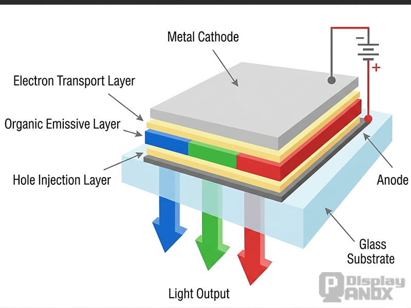
3. Organic Layer Evaporation
This is universally recognized as the most difficult and critical stage of AMOLED manufacturing.
In a high-vacuum environment (10^-5 to 10^-7 Torr), organic luminescent materials are heated until they vaporize, depositing molecularly onto the substrate to form thin films.
-
Core Equipment: Vacuum evaporation machines (often dominated by Canon Tokki, costing $100-$200 million per unit) are paired with Fine Metal Masks (FMM). These FMMs, often sourced from companies like Dai Nippon Printing, cost between $500,000 and $1,000,000 per set.
-
The Material System: The screen relies on precise mixes of Red (e.g., Ir(piq)3), Green (e.g., Ir(ppy)3), and Blue organic materials, alongside Hole and Electron Transport Layers (HTL/ETL).
-
Technical Hurdles: Manufacturers must achieve perfect pixel alignment (±2μm precision) to prevent color mixing, maintain uniform luminance across the board (under 2% variance), and manage poor material utilization (FMM utilization is historically only 5-10%).
4. Encapsulation Process
Organic light-emitting materials degrade rapidly when exposed to oxygen or moisture. Therefore, hermetic encapsulation is essential for screen longevity.
-
Thin-Film Encapsulation (TFE): The standard for flexible displays. It alternatingly layers inorganic materials (like Al2O3 and SiNx) to block moisture and organic materials (like PI) for flexibility.
-
Strict Metrics: The barrier must achieve a Water Vapor Transmission Rate (WVTR) of less than 10^-6 g/m²/day and an Oxygen Transmission Rate (OTR) of less than 10^-5 cc/m²/day.
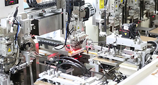
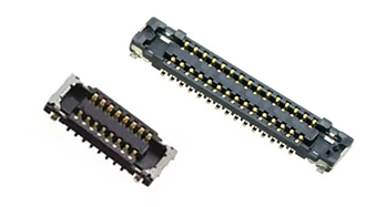
5. Module Assembly and Testing
The final stage transforms the sealed glass/film into a functional display panel. The process flows from panel cutting and polarizer attachment to connecting the driver IC (COF/COG bonding with ±3μm precision) and PCB. Strict optical inspections and aging tests are conducted to ensure zero defects before shipping. The entire cycle from bare substrate to finished module takes roughly 20 to 30 days.
Manufacturing Barriers and Yield Economics
Yield rate is the lifeblood of AMOLED profitability. Because the process is so intricate, a failure at any stage ruins the entire panel.
-
A 30% yield rate results in production costs multiplying by 3.3x, causing severe losses.
-
A 50% yield rate is roughly the breakeven point.
-
A 70% yield rate ensures normal profitability, while 85% is considered an excellent, industry-leading standard.
The Blue Light Bottleneck: One of the most persistent challenges in organic material science is the lifespan of blue sub-pixels. While red OLED materials can last over 100,000 hours and green over 80,000 hours, blue materials historically degrade after just 20,000 hours. Furthermore, the luminous efficiency of blue light is only about 30% compared to red and green. This discrepancy is the root cause of OLED "burn-in" and color shifting over time.
2026 Industry Trends: What's Next for AMOLED?
As we move through 2026, several manufacturing leaps are actively reshaping the market:
The Shift to Generation 8.6 Fabs
The push for IT-OLEDs (laptops and tablets) has necessitated larger motherglass substrates. Gen 8.6 lines are currently rolling out, significantly improving cutting efficiency. While Gen 6 lines yield only about 60% utilization for smartphone cuts, Gen 8.6 pushes that to 90%, driving manufacturing costs down by an estimated 15-20%.
Inkjet Printing OLED
To combat the low material utilization (5-10%) of traditional vacuum evaporation, manufacturers are advancing Inkjet Printing (IJP) technology. IJP drastically increases material utilization to over 90% and lowers equipment costs by roughly 30%.
The Rise of Micro OLED for AR/VR
Micro OLED, which combines a silicon wafer backplane with an OLED emissive layer, is seeing explosive growth for spatial computing. Because it abandons traditional glass for silicon, it can achieve astonishing pixel densities exceeding 4000 PPI with microsecond response times—vastly outperforming the 400-500 PPI of standard AMOLEDs.
FAQ: AMOLED Manufacturing
Q: How long does it take to manufacture a single AMOLED panel?
A: The entire end-to-end manufacturing cycle takes approximately 20 to 30 days. This includes substrate preparation (3-5 days), TFT backplane fabrication (10-15 days), organic evaporation (2-3 days), encapsulation (1-2 days), and final module assembly and testing (3-5 days).
Q: Why is blue light a problem in AMOLED screens?
A: Blue organic light-emitting materials have a naturally shorter lifespan (around 20,000 hours) compared to red (>100,000 hours) and green (>80,000 hours). Because the blue pixels die faster, the display can suffer from color shifting or "burn-in" over extended use.
Q: What is the difference between Rigid and Flexible AMOLED manufacturing?
A: The primary difference lies in the base substrate and the encapsulation method. Rigid panels use flat glass substrates and traditional glass/UV glue encapsulation. Flexible panels use a bendable Polyimide (PI) film as the substrate and utilize Thin-Film Encapsulation (TFE)—a complex layering of organic and inorganic materials—to protect the screen while allowing it to bend.
Q: Why are AMOLED screens so expensive to produce?
A: The high cost stems from the extreme precision required and the cost of capital equipment. For instance, the evaporation machines required for depositing organic materials can cost $100-$200 million per unit. Furthermore, any defect in the complex process destroys the panel, meaning yield rate heavily impacts the final cost per unit.
Ready to integrate these cutting-edge displays into your next project? Browse our latest panels on the AMOLED product page.